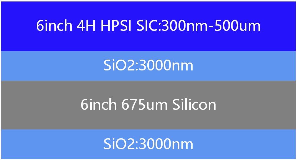
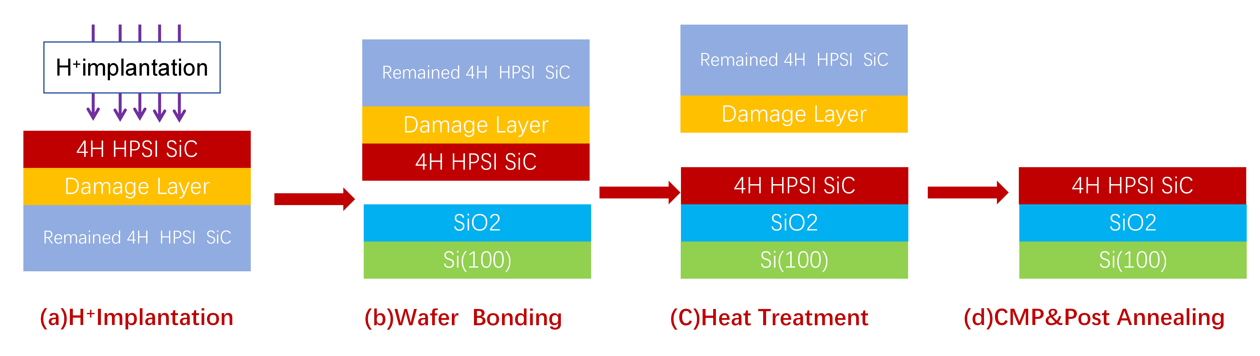
OMedaSemi develop 4-6 inch SICOI wafers (silicon carbide on insulator wafers). The wafers use Direct Bonding(hydropholic bonding) to bond thermal oxide wafers and 4H high-purity semi-insulating silicon carbide wafers together, and then control the thickness to the thickness you need through ion implantation, annealing, thinning or direct thinning and CMP polishing. ion implantation and direct CMP and thinning have their own advantages and disadvantages.
Optical Data we provide:Refractive Index and Absorption Data For Photonics integrated Circuit
Quantity that we shipped to Clients:20PCS
Data that we have ship to clients
Capbility
Based on SMARTCUT process, this method can provide good uniformity but bad optical performance so mainly for MEMS
Film thickness: 50nm-20um
Film thickness uniformity :+-20nm
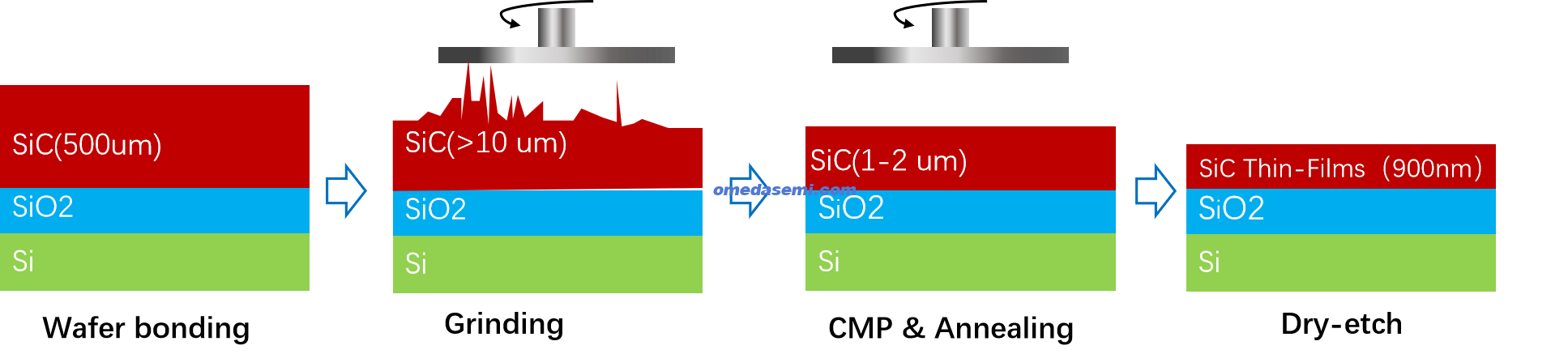
Based on Grinding+CMP process,this method can provide not so good uniformity but good optical performance so mainly for Photonics and Quantum
Film thickness range: 200nm-any thickness
Film thickness uniformity: +-100nm
Optical Data for you to Simulation
 Refractive index and Absorption of Bulk crystal and Thin Film Crystal.zip
Related paper:(Quantum Photonics MEMS)
Visible and Near-infrared Microdisk Resonators on a 4H-Silicon-Carbide-on-Insulator Platform.pdf
Spontaneous Parametric Down-Conversion in 4H-SiC.pdf
Dopant Selective Photoelectrochemical Etching of SiC.pdf
Multiemitter cavity quantum electrodynamics in 4H-silicon carbide-on-insulator photonics.pdf
Visible to Mid-infrared Supercontinuum Generation in 4H Silicon Carbide Nanophotonic Waveguides.pdf
Supercontinuum Spanning 2.8 Octaves in 4H-Silicon-Carbide Waveguides.pdf
Self-Referenced_Mid-Infrared_Frequency_Comb_Using_a_Silicon-Carbide_Nanophotonic_Waveguide.pdf
Tunable cavity coupling to spin defects in 4H-silicon-carbide-on-insulator platform.pdf
Optical parametric oscillation in silicon carbide.pdf
Room-temperature waveguide integrated quantum register in a semiconductor photonic platform.pdf
Low Dissipation Nanomechanical Devices from Monocrystalline Silicon Carbide.pdf
Mesoscopic cavity quantum electrodynamics with phase-disordered emitters.pdf
Two-Emitter Multimode Cavity Quantum Electrodynamics.pdf
4H-silicon-carbide-on-insulator for integrated quantum and nonlinear photonics.pdf
Related paper:(MEMS)
MEMS Thermocouple Sensor Based on 4H-Silicon-Carbide-On-Insulator (4H-SiCOI).pdf
4H-Silicon Carbide as an Acoustic Material for MEMS.pdf
 Piezoresistive 4H-Silicon Carbide SiC pressure sensor.pdf
Demonstration_of_SiC-on-Insulator_Substrate_with_S.pdf
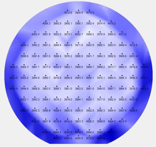
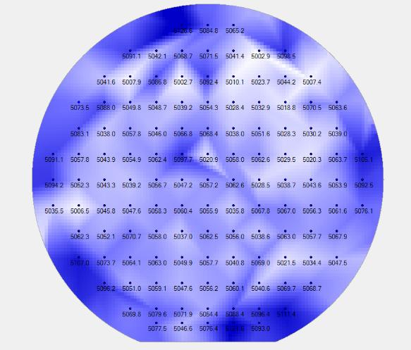
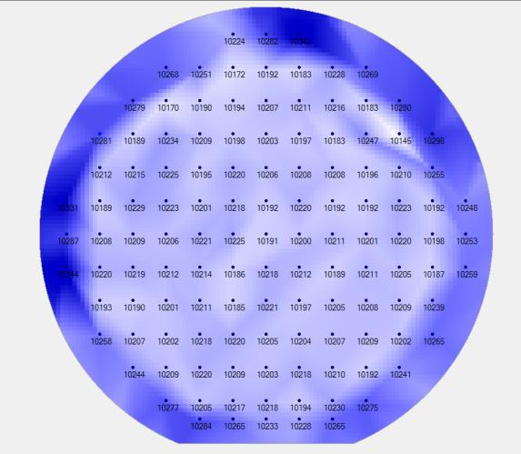
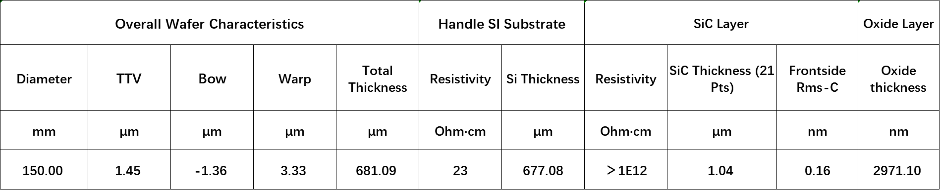
Test Data
Wafer 1:-400nm
 Wafer 2:-500nm
Wafer 3--1um
OMeda (Shanghai Omedasemi Co.,Ltd) was founded in 2021 by 3 doctors with more than 10 years of experience in nanpfabrication. It currently has 15 employees and has rich experience in nanofabrication (coating, lithography, etching, two-photon printing, bonding) and other processes. We support nanofabrication of 4/6/8-inch wafers.