OMedasemi provide SOI wafers
Now we can provide 4inch (thick film >5um ) ,6inch (thick film>5um and Thin film>150nm ) ,8inch (thick film>5um and Thin film>150nm ) ,12inch (thick film>5um and Thin film>150nm )
The fabrication process of Silicon-on-Insulator (SOI) wafers involves several key steps. SOI wafers are used in various semiconductor applications, including Photonics integrated Circuit,advanced integrated circuits (ICs), RF devices, and MEMS.


4inch 6inch 8inch 12inch
Capability introduction (must read):
Size: 4 inches, 6 inches, 8 inches ,12inch
Device layer tolerance: +-10nm (6inch ordinary level), +-20nm (8inch ordinary level), +-5nm (high precision with trimming process ,Know more:Trimming Process Introduction)
Top silicon layer thickness: 30nm-1500nm (SMARTCUT process) Greater than 600nm (thinning and polishing + finishing process, because the thinning and polishing process is used, the thickness can be very thick)
Thermal oxide layer thickness: 50nm-500nm (dry thermal oxide), 500nm-20um (wet thermal oxide)
Substrate thickness: customizable
Application:
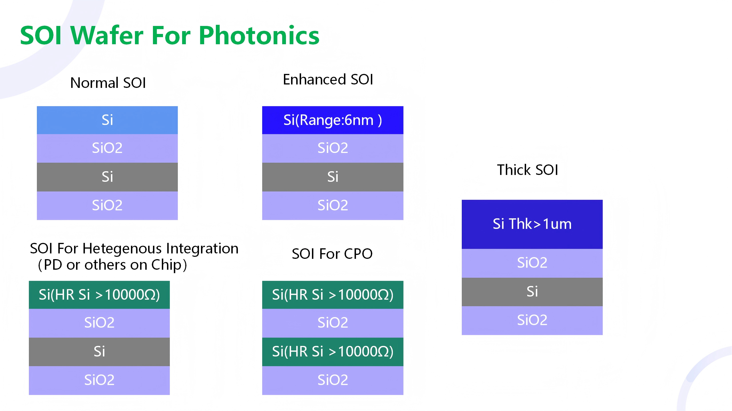
SOI Wafer For Photonics Integrated Circuit (Smartcut):
220nmSi-3umSiO2-525um/675um/725um Si (Thin film silicon photonics) --in Stock
3umSi-3umSiO2-525um/675um/725um Si (Thick film silicon photonics) --in Stock
Data we provide:Refractive Index and Absorption Data For Photonics integrated Circuit
the mostly used is 220nmSi-3umSiO2-525um/675um/725um Si (Thin film silicon photonics) and 3umSi-3umSiO2-525um/675um/725um Si (Thick film silicon photonics) and also other customized spec soi wafer .
Innovation:Also recently ,SOI wafer for photonics with high resisitivity silicon is more and more popular ,OMedaSemi also can provide this kind SOi wafer ,the device layer and handle layer's resisitivity is bigger than 10k ohm*cm.
111 Oriented SOI Wafers for GaN Epitaxy in Power Devices - GaN-SOI
Our company has successfully developed 111-orientated SOI wafers for RF GaN epitaxy.
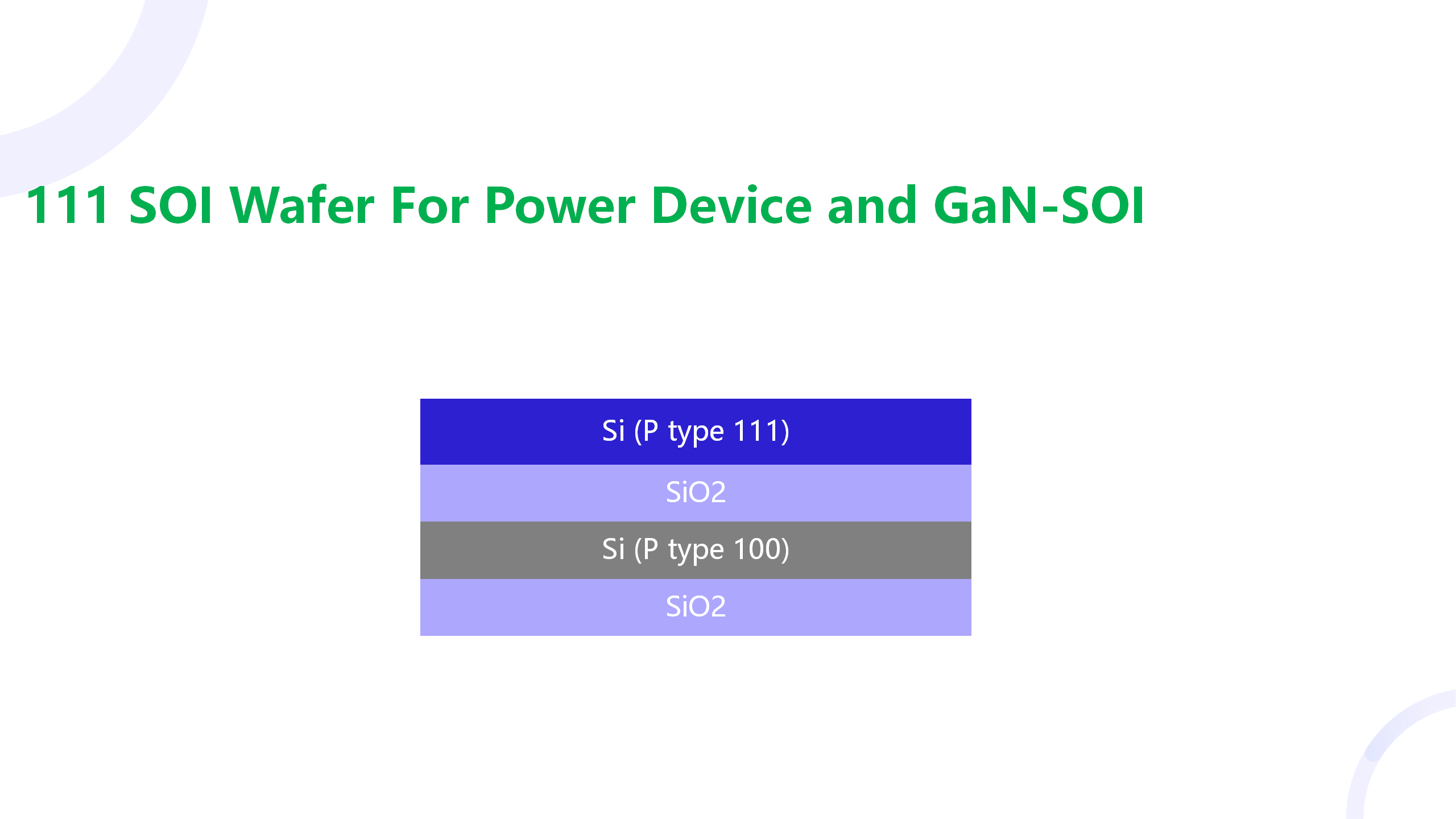
Advantages of Using 111-Oriented SOI Substrates for GaN Epitaxy in Power GaN Devices
"Integrating multiple GaN power devices onto a single chip significantly reduces the size of the power loop, eliminates interconnect parasitics, and reduces assembly complexity. In lateral GaN-on-Si processes, placing multiple power devices on a single chip is straightforward. However, when GaN devices operate at high source-to-substrate voltages, back-gating and threshold voltage shifts can lead to uneven current distribution, reducing efficiency. To fully isolate devices on the same substrate, GaN-on-SOI technology is essential to eliminate back-gating effects and reduce parasitic capacitance."
"Power devices in GaN-on-Si" Monolithic integration on a substrate is hampered by crosstalk between devices and the "backgating" effect caused by substrate contacts. One solution to suppress crosstalk and backgating is to use SOI (silicon-on-insulator) substrates combined with trench isolation. GaN-on-Si devices exhibit a "backganting" effect, in which the silicon substrate affects the electrical characteristics of the channel in the GaN-on-Si structure. This effect can lead to instabilities in threshold voltage and leakage current, thus affecting device performance and reliability. Another solution is to use an engineered substrate with a polysilicon AlN core, commercially available as QST® (QROMIS Substrate Technology). The relatively high price of QST® substrates has hindered their widespread adoption. Recently, there has been significant interest in GaN-on-Sapphire, which can also be used as a substrate for GaN monolithic integrated circuits. A drawback of GaN-on-Sapphire is the low thermal conductivity of sapphire substrates. Therefore, SOI substrates offer a good trade-off between low cost and high performance for monolithic circuits.
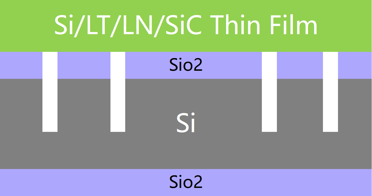
Cavity SOI for MEMS(Smartcut)
Our company can provide CavitySOI wafers. To ensure the quality of the top device layer, we maintain a maximum cavity-to-device layer thickness ratio of 45:1. Furthermore, our advantage lies in our ability to produce ultra-high-precision cavities. The smallest line width achieved by other leading CavitySOI companies is 2µm, achieved using contact lithography machines. Our company uses stepper lithography to create handle wafer patterns. Combined with etching processes, we can produce cavities with minimum line widths of 180nm .
Also we extend the material from silicon to lithium niobate ,lithium tantalate and silicon carbide
SOI wafers for RF devices, RF-SOI
Structure: Si-Poly Si (Trap Rich Layer)-SiO2-Si
Our company can provide SOI wafers for RF devices in 6-inch and 8-inch sizes. The handle layer is generally high-resistance silicon, and the trap rich layer is generally LPCVD poly Si. The final thickness of this layer can be 1300nm.
Ultra Thin Device and Box layer SOI wafer (FDSOI)(Smartcut+Trimming)
For example:30nmSi-3umSiO2-675um Si(Range:5.9nm)

Ultra Thick Device and Box layer SOI wafer:(Grinding+CMP+trimming)
For example:20umSi-3umSio2-675umSi(Range:176.8nm)

UltraThin-SOI (UltraThin-SOI)
Structure: Si-SiO2-Si
Using our patented technology, we can produce SOI with a total thickness (Si+SiO2+Si) as thin as 150µm.
Business process (must read):
#1: Client determines what it needs for each layer (a, film thickness, b, silicon resistivity, crystal orientation, etc. c, wafer size)
#2: Supplier issues a specification sheet according to Client's requirements and sends it to Client for confirmation
#3: Client confirms that the specification sheet is correct, signs the contract, and processes
About the cycle: The general SOI processing cycle is 1-2 months
About the price: The minimum order is 1 piece, the price is expensive, it is recommended to purchase 5 pieces at a time, the price is more affordable, contact the editor to obtain the price
About product quality: Processing is carried out in full accordance with the specification sheet, and a shipping report is issued after processing, with detailed information such as TTVBOWWRAP, and the product quality is stable and reliable.
About payment: Cash on delivery is supported, 50% prepayment and 50% cash on delivery are recommended
Advantages:
We have a complete production line for bonding, ion implantation, annealing, polishing and high-precision trimming, so we have strong custom processing capabilities. Unlike the arrogant attitude of the world's mainstream SOI manufacturers, we accept orders for one SOI wafer. At the same time, our delivery speed is relatively fast. The production process only takes 3-4 weeks.
Customization process:
1. Silicon wafer preparation (generally, the customization of silicon wafers takes about 3 weeks, if it is inventory, there is no need for silicon wafer customization time)
2. Double-sided polishing
3. Ion implantation
4. Bonding
5. Annealing
6. CMP polishing
7. Trim finishing (2-7 processes take about 4-6 weeks)


Stock List
Please click the lick to download the list of SOI wafer Stock
### Fabrication Process of SOI Wafers:
1. **Starting Material Selection:**
- **Substrate Wafer:** The base wafer is typically a standard silicon wafer.
- **Insulator Layer:** The most common insulator used is silicon dioxide (SiO2), though other materials can be used as well.
2. **Bonding Techniques:**
- **Wafer Bonding (SOI):** The silicon wafer is bonded to a layer of silicon dioxide. This is done through processes such as direct bonding or fusion bonding, where two wafers are brought into contact and heat/pressure is applied to form a strong bond.
- **Smart Cut Method:** This is a widely used method for producing SOI wafers, where a thin layer of silicon is implanted with hydrogen ions and then bonded to an oxidized wafer. The bonded assembly is then subjected to heat, causing the implanted layer to cleave, forming a thin silicon layer atop an insulating layer.
3. **Layer Thickness Control:**
- The thickness of the silicon layer and the insulating layer must be precisely controlled. This can be achieved through various techniques, including ion implantation and etching.
4. **Wafer Thinning:**
- If necessary, the SOI wafer may undergo further thinning to achieve the desired dimensions for applications.
5. **Surface Cleaning and Finishing:**
- The wafers are thoroughly cleaned to remove any contaminants. A final polish may also be applied to ensure a smooth surface.
6. **Characterization and Quality Control:**
- The wafers undergo various tests to ensure they meet the required specifications, including electrical and physical characteristics.
### Applications of SOI Wafers:
1. **High-Performance Integrated Circuits (ICs):**
- SOI technology enhances the performance of high-speed and low-power devices, reducing parasitic capacitance and thus improving switching speeds.
2. **Radio Frequency (RF) Devices:**
- SOI wafers are used in RF applications due to their higher electromechanical performance and lower noise figures.
3. **Ultra-Low Power Devices:**
- SOI technology is ideal for low-power applications, such as IoT devices and mobile electronics, as it minimizes leakage currents.
4. **Memory Devices:**
- SOI wafers are employed in manufacturing certain types of memory, including SRAM and Flash memory, to improve performance and reduce power consumption.
5. **Micro-Electro-Mechanical Systems (MEMS):**
- SOI wafers are also used in MEMS fabrication, allowing for the integration of mechanical and electronic components on a single chip.
6. **Solar Cells:**
- Certain types of SOI wafers are investigated for use in solar cells, utilizing their lightweight and efficient characteristics.
By leveraging the properties of SOI wafers, manufacturers can create devices that are faster, more efficient, and capable of meeting the demands of various modern applications.
OMeda (Shanghai Omedasemi Co.,Ltd) was founded in 2021 by 3 doctors with more than 10 years of experience in nanpfabrication. It currently has 15 employees and has rich experience in nanofabrication (coating, lithography, etching, two-photon printing, bonding) and other processes. We support nanofabrication of 4/6/8-inch wafers.