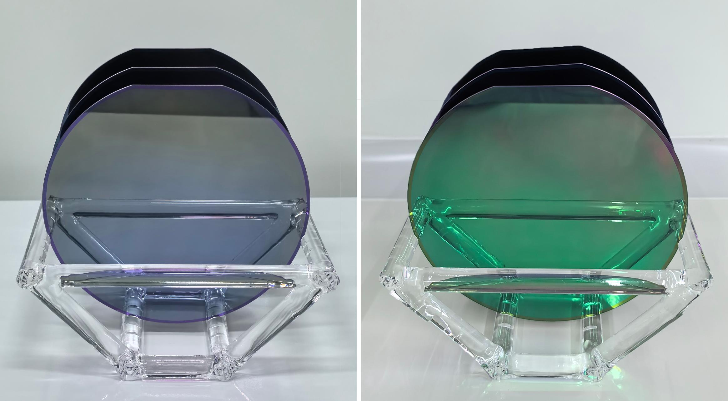
OMedaSemi provide poi(Piezoelectric on Insulator) wafer,we have both hydrophilic bonding and Surface Active Bonding . Not only LNOI and LTOI wafer , we also can provide LN/LT-SIC,LN/LT-Quartz,LN-SiO2-Sic

Application:SAW surface acoustic wave device--POI wafer
Type:
*IHP-SAW Acoustic grade LTOI
*TF-SAW Acoustic grade LTOI
*LTOI
*LN/LT-SIC
*LN/LT-Quartz
Size: 4 inches 6 inches 8 inches
Crystal Orientation: Y cut-Y128, Y36 (SAW), Z cut (SAW) and more
Processing technology: hydrophilic bonding + annealing, surface activation bonding
Customized processing: In addition to standard LNOI wafers, we also provide customized processing services for LNOI wafers.
Our advantages: full process and comprehensive processing capabilities
*Ion implantation
*Thinning and polishing
*Surface activation bonding
*Hydrophilic bonding
*Annealing
*Grinding+CMP
Comprehensive processing capabilities can provide you with fast and efficient customized processing services.
Related Paper:
Evolution of SAW and BAW Devices Using Thin LiTaO3 and LiNbO3
Acoustic Devices PAW SAW and BAW using Wafer Bonding Technology
OMeda (Shanghai Omedasemi Co.,Ltd) was founded in 2021 by 3 doctors with more than 10 years of experience in nanpfabrication. It currently has 15 employees and has rich experience in nanofabrication (coating, lithography, etching, two-photon printing, bonding) and other processes. We support nanofabrication of 4/6/8-inch wafers.