Hello, this page mainly introduces deep silicon etching. First, we will introduce the equipment we use.
Project we have done before :
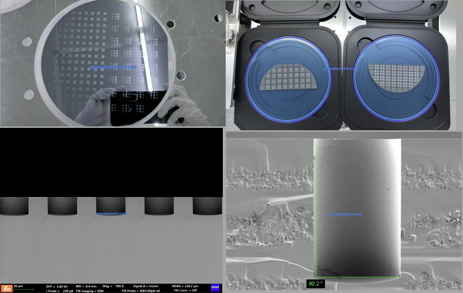
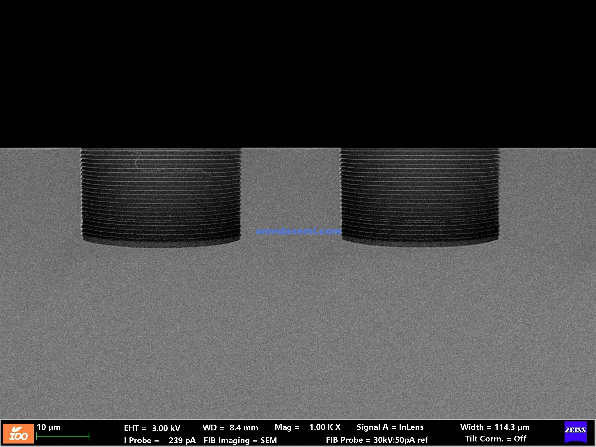
Equipment Name: Deep Reactive Plasma Etching System
Brand Model: SPTS Omega LPX Rapier (4-8 inches) AMAT (12 inches)
Main Function: Etching various silicon-based materials, especially suitable for high aspect ratio etching processes
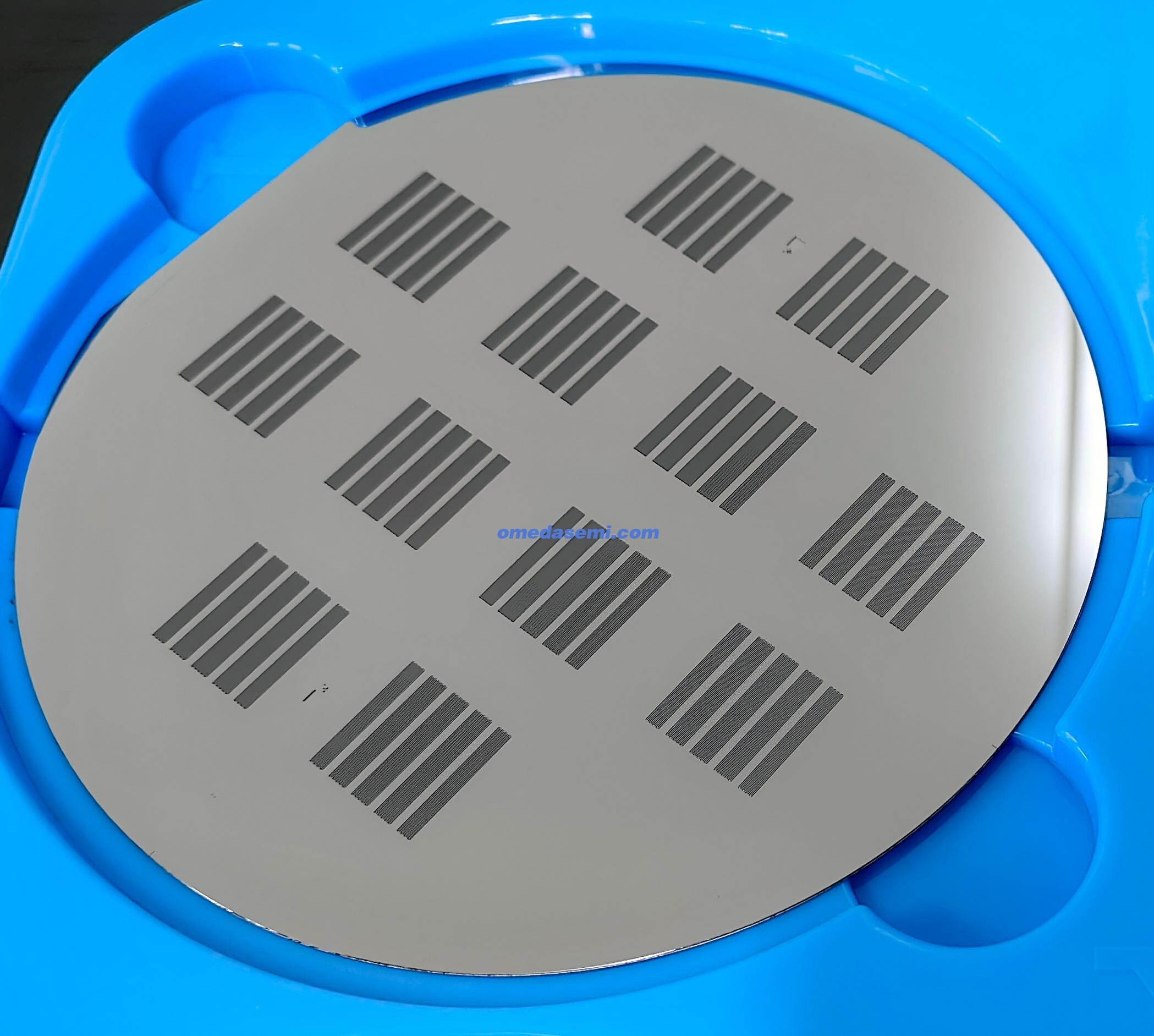
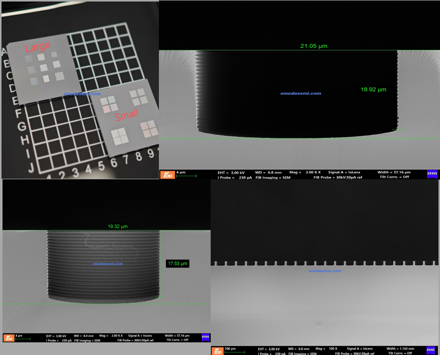
Size: Up to 12 inches
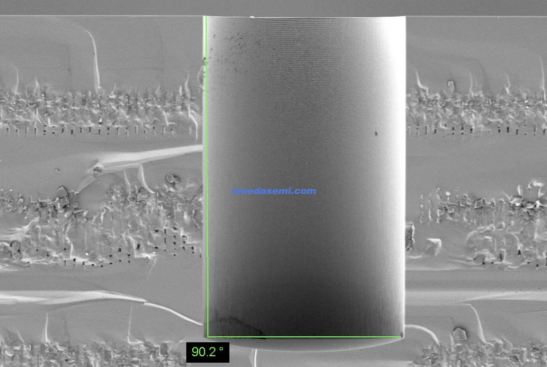
Maximum aspect ratio: 50:1
Etching verticality: 90 degrees
Maximum Etch Depth: 675µm
Applications:
#1: Backside cavity opening for acoustic wave filters and MEMS sensors
#2: Deep silicon etching in TSV processes
#3: Silicon channel fabrication
Our Advantages:
Advanced Photolithography: Introduction to Photolithography
The first step before deep silicon etching is photolithography. In addition to advanced deep silicon etching processes, we also possess advanced photolithography technologies, ranging from the smallest node to the smallest node in wafer-level processing. 150nm, with wafer-level processing down to 50nm.
Combining with bonding processes creates more possibilities: Introduction to bonding
Our company can bond structured wafers after deep silicon etching to various materials, including glass, silicon, and silicon carbide.
Combining with various coating processes creates more possibilities: Introduction to coating
For example : Coating multilayer dielectric mirrors to develop hollow-core optical waveguides
Case Studies:

OMeda (Shanghai Omedasemi Co.,Ltd) was founded in 2021 by 3 doctors with more than 10 years of experience in nanpfabrication. It currently has 15 employees and has rich experience in nanofabrication (coating, lithography, etching, two-photon printing, bonding) and other processes. We support nanofabrication of 4/6/8-inch wafers.