Gas Cluster Ion Beam Trimming Machine
OMedaSemi provide Gas Cluster Ion Beam(GCIB) Trimming Machine We can provide fully automatic GCIB triM machine(SAB9510:Beam Size FWHM<5mm) for mass production and semi automatic machine(SAB9500:Beam Size FWHM<10mm) for Research .
Gas Cluster Ion Beam VS Reactive Ion Beam
#Lower Temperature(total process is in room temperature environment)
#No Deep implantation and Less Damage(avoid the damage to film)
Beam Size:
Smaller Beam Size can correct the ununiformity in a smaller area and get the ultra uniform surface .
| Mode | SAB9510--Fully automatic cluster plasma TRIM machine |
| Wafer size | ≤8 inch |
| Material | Diamond.SIC,InP,Glass,Si,GaN,AlN,Al2O3,LN,LT,Ga2O3.,etc |
Loading mode | Cassette automatic loading and unloading |
Wafer calibration | Aligner |
Removal efficiency | 800 Å*cm²/s @Si |
Supported process gases | Ar/SF6/O2/HeOr other mixed gases |
Beam intensity | >100μA @Ar |
Beam spot size | FWHM<5mm |
Cluster ion energy | 20/60keV |
| Mode | SAB9500-Semi Automatic cluster plasma TRIM machine |
| Wafer Size | 4-12 inch (size can be customized) |
Wafer load | Manual |
Transmission | Manual/Customized Tooling |
Removal efficiency | 70 Å*cm²/s @SiO₂ |
process gas | Ar/SF6/O2/He or other mixed gases |
Beam intensity | >100μA @Ar |
Beam spot size | FWHM<10mm |
Cluster ion energy | 20/60keV |
Application:
#Improve the uniformity of the wafer surface film thickness
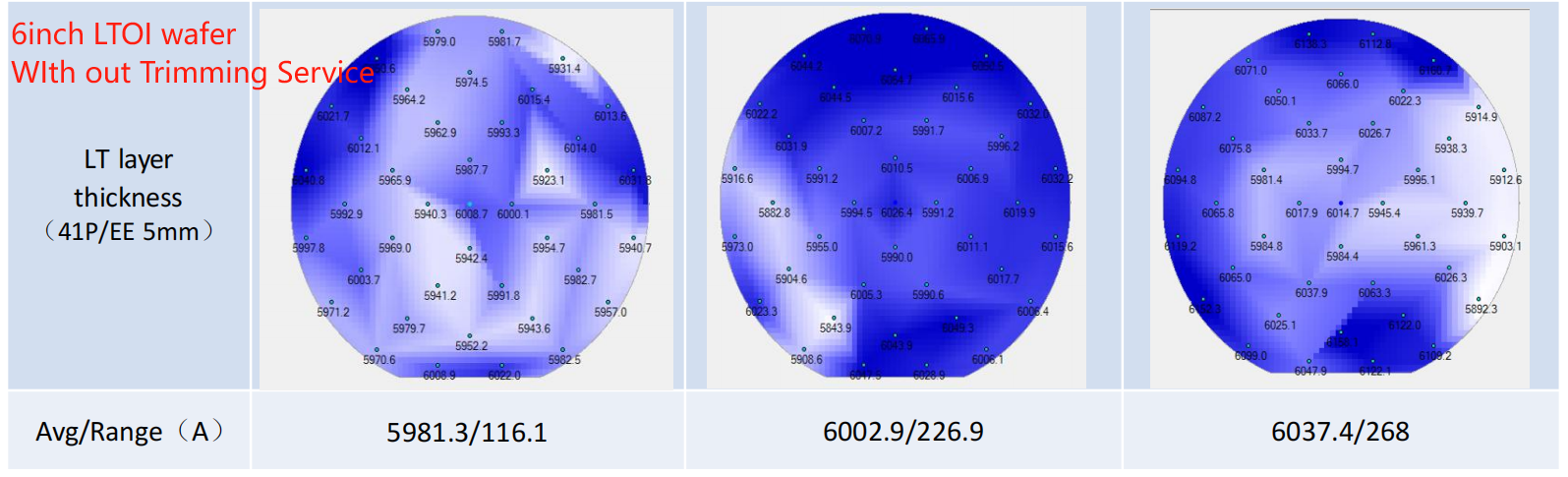
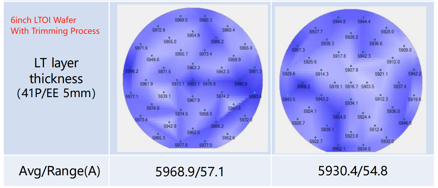
For example: SOI LNOI LTOI SICOI
6 inch LTOI Wafer Without Trimming Service: Range 100A-200A
6 inch LTOI Wafer With Trimming Process:Range:<57A
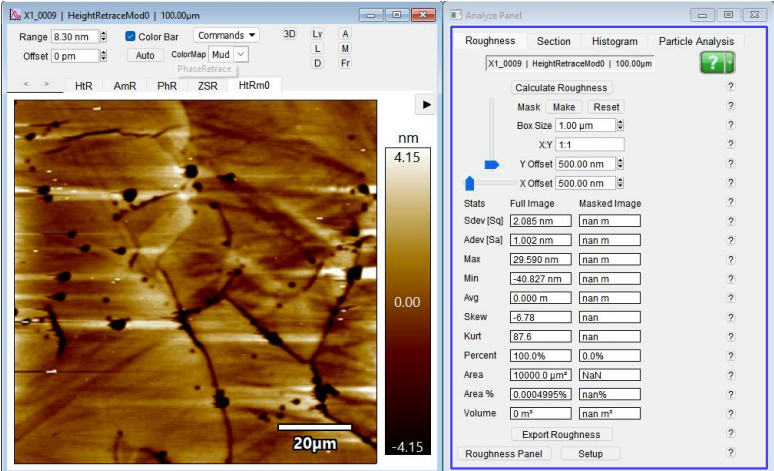
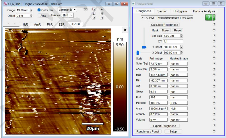
#Reduce the roughness of the substrate surface
For example:Diamond,InP SiC Sapphire SIlicon Glass,crystal,and more , Surface Polishing to get ultra low roughness data
#ultra-smooth surface processing
# surface trim, ultra-precision trim ofsemiconductor films
# non-contact polishing of super-hard materials and curved surfaces
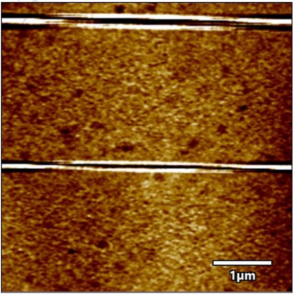
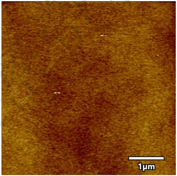
Diamond Polishing
(Before:Ra1.17nm After:Ra0.42nm)(5um*5um)
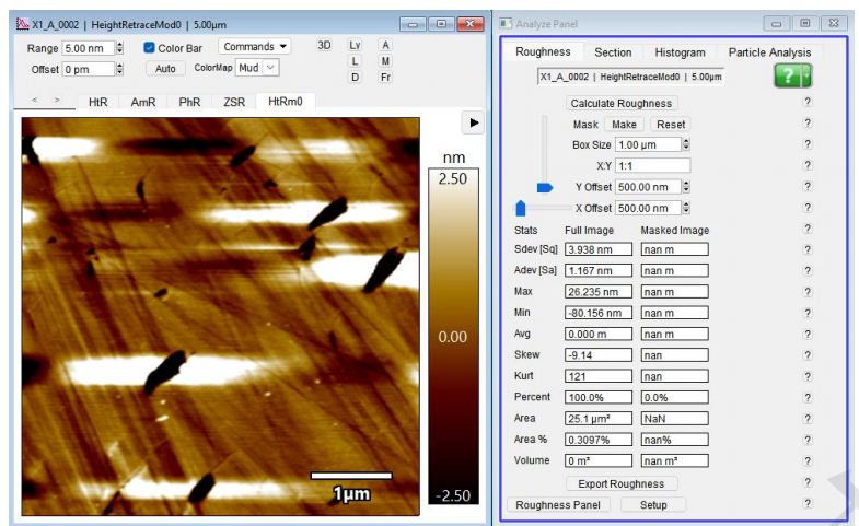
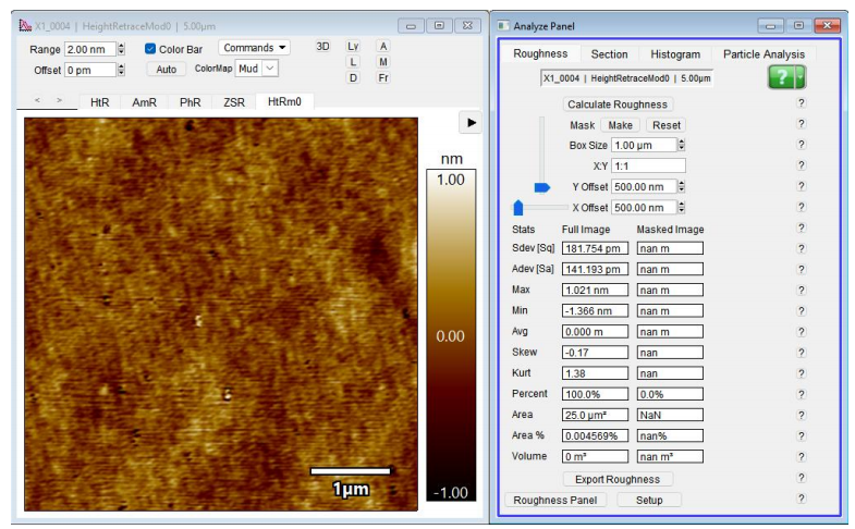
(Before:Ra2.68nm After:Ra1nm)(100um*100um)
Lithium Niobate Polishing
(Before:Ra0.72nm After:Ra0.11nm)(5um*5um)
Market:
#Semiconductor
RF Filter (SAW FBAR TCSAW SMR-BAW)
Photonics Waveguide
#Optics
Ultra low roughness and ultra flat polishing
Gas Cluster Ion Beam (GCIB) Trimming Technology is a specialized surface modification and processing technique that uses clusters of gas ions to treat the surfaces of materials with high precision. Here’s an overview of its principle and applications:
GCIB technology involves the use of gas clusters, which are groups of gas atoms (usually noble gases like argon or helium) that are ionized and accelerated to high energies. These ionized gas clusters are then directed at a material’s surface.
The primary principle behind GCIB is that when these ion clusters impact the surface of a material, they interact with the surface atoms. The energy from the cluster bombardment is transferred to the material, leading to the removal or modification of atoms from the surface. This process can result in precise surface etching, cleaning, polishing, or modification of material properties.
Key steps in the GCIB process:
Cluster Formation: Gas atoms (like argon or helium) are clustered together using techniques like supersonic expansion or cryogenic cooling.
Ionization: The clusters are ionized to become positively charged ions.
Acceleration: The ions are accelerated using an electric field to achieve high kinetic energy.
Surface Interaction: The ions impact the target material’s surface, modifying the material at the atomic or molecular level.
Semiconductor Industry:
Etching and Cleaning: GCIB technology is widely used in semiconductor fabrication for etching fine features and cleaning surfaces. It allows for precise trimming of microstructures without causing damage to surrounding areas.
Surface Modification: GCIB is used to modify surface properties like roughness, energy, and adhesion to enhance the performance of semiconductor components.
Material Science:
Surface Smoothing: It is used to smooth rough surfaces of materials at the nanometer scale. This is particularly important in applications where surface uniformity is crucial.
Polishing: GCIB can be used for fine polishing of hard materials like metals, ceramics, and thin films, especially when high precision is required.
Optics and Thin Films:
Surface Treatment: GCIB is employed to treat optical surfaces, remove contaminants, and enhance the optical properties of thin films and coatings.
Trimming of Thin Films: It is used for thinning or trimming films to achieve exact thicknesses or desired properties.
Nanotechnology:
Nanostructuring: GCIB can be used for the creation of nanostructures on material surfaces, enabling the development of new nanomaterials and nanodevices.
Patterning: It is also useful in patterning techniques for nanoelectronics and nano-optics.
Material Hardening and Modifications:
GCIB can induce changes in the microstructure of materials, such as surface hardening, without affecting the bulk properties of the material.
It can be used for modifying surface stress, introducing controlled damage, or creating thin coatings that increase wear resistance.
High Precision: GCIB technology allows for extremely fine and precise modifications of material surfaces, essential in fields like semiconductor manufacturing and optics.
Minimal Heat Effects: Unlike other ion beam techniques, GCIB causes minimal heating of the material, preventing thermal damage.
Minimal Surface Damage: The clustered ions impact the material in a way that minimizes unwanted collateral damage to the substrate.
Versatility: GCIB can be used on a wide variety of materials including metals, polymers, semiconductors, and ceramics.
In summary, GCIB technology is a powerful and versatile tool used for surface modification and trimming in high-tech industries. It excels in applications requiring precision and minimal damage to the material, making it an invaluable technique in modern material processing.
OMeda (Shanghai Omedasemi Co.,Ltd) was founded in 2021 by 3 doctors with more than 10 years of experience in nanpfabrication. It currently has 15 employees and has rich experience in nanofabrication (coating, lithography, etching, two-photon printing, bonding) and other processes. We support nanofabrication of 4/6/8-inch wafers.