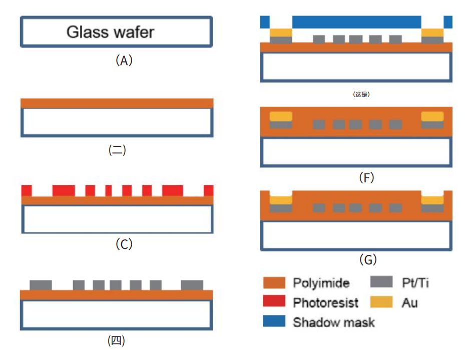
Principle:
Flexible electrodes manufactured using MEMS (micro-electromechanical systems) technology are microelectronic components with good flexibility and conductivity. Its manufacturing process involves multiple precision processing steps, combining traditional semiconductor manufacturing technology and flexible material processing technology. The following is a detailed manufacturing process, advantages and application scenarios:
Manufacturing process

1. Substrate preparation:
Selection of substrate: Polymer films such as polyimide (PI), polyethylene terephthalate (PET), etc. are usually used as flexible substrates.
Cleaning the substrate: Use chemical solvents to clean the substrate to ensure that there are no contaminants on its surface.
2. Deposition of conductive layer:
Sputtering or evaporation of metal: Deposit a layer of metal (such as gold, platinum, silver, aluminum, etc.) on the substrate to form a conductive layer. Sputtering and evaporation are commonly used methods.
Chemical vapor deposition (CVD): CVD is sometimes used to deposit conductive materials.
3. Photolithography:
Photoresist coating: Coat a layer of photoresist on the conductive layer.
Exposure and development: Use a mask to expose the pattern to the photoresist through ultraviolet light, and then develop to reveal the pattern.
4. Etching:
Dry etching: Use plasma etching technology to remove the metal parts not protected by the photoresist.
Wet etching: Use chemical solutions (such as acids or alkalis) to etch the metal areas not covered by the photoresist.
5. Removal of photoresist:
Use organic solvents or plasma treatment to remove the residual photoresist and retain the patterned metal layer.
6. Encapsulation and protective layer:
Coating a protective layer: Coat a layer of insulating and protective material (such as polyimide) on the surface of the flexible electrode to improve its mechanical strength and environmental resistance.
Heat treatment: The protective layer is cured through a heat treatment step to increase its stability.
Advantages:
1. Flexibility: It can adapt to bending, stretching and twisting, and is suitable for various complex surfaces.
2. Lightweight: Lightweight, suitable for portable and wearable devices.
3. High conductivity: A wide range of conductive materials can achieve efficient electrical conduction.
4. Good biocompatibility: The use of appropriate materials can ensure safety and effectiveness in biomedical applications.
5. Mass production: MEMS technology is suitable for large-scale production and can reduce manufacturing costs.
Application scenarios:
1. Wearable devices:
Smart bracelets and watches: used for biological signal detection (such as heart rate, blood oxygen saturation).
Flexible display screens: As electrode materials for display screens, they provide flexible touch functions.
2. Biomedical devices:
Brain-computer interface: Flexible electrodes can be implanted in the brain for the collection and stimulation of neural signals.
Pacemakers and electrocardiogram electrodes: used for cardiac monitoring and treatment equipment.
3. Sensors:
Pressure and strain sensors: used to monitor pressure, stress and deformation, and are used in health monitoring, motion tracking, etc.
Chemical and biological sensors: used to detect chemicals or biomolecules in the environment.
4. Electronic skin:
Human-machine interaction: used for tactile sensing of robots, enabling them to sense the external environment and achieve sensitive touch.
Prosthetic perception: used in prostheses to give them perception capabilities and enhance the user experience.
5. Flexible electronics:
Flexible circuit boards: used in various electronic devices that require flexible connections.
Solar cells: Flexible electrodes are used in thin-film solar cells to improve their installation convenience and scope of application.
Flexible electrodes manufactured using MEMS technology have shown important value in modern technology with their unique advantages and broad application prospects.
OMeda (Shanghai Omedasemi Co.,Ltd) was founded in 2021 by 3 doctors with more than 10 years of experience in nanpfabrication. It currently has 15 employees and has rich experience in nanofabrication (coating, lithography, etching, two-photon printing, bonding) and other processes. We support nanofabrication of 4/6/8-inch wafers.