Silicon Photonics Fabrication Capbility
SIZE:6inch
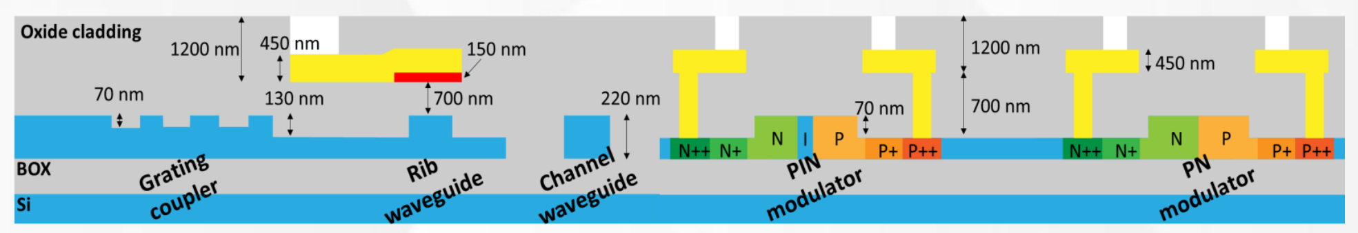
Min CD SIZE:180nm
Etching Depth and Uniformity:70nm/130nm/220nm+-10nm
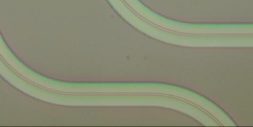
Waveguide loss:Straight waveguide loss 2-3 dB/cm
*6 inches 24 shots fabrication:

Overlay error ±50 nm
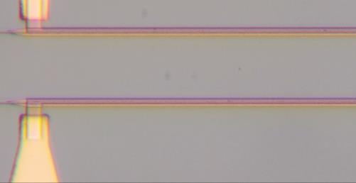
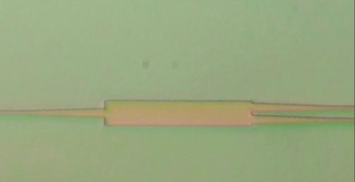
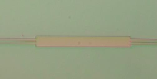
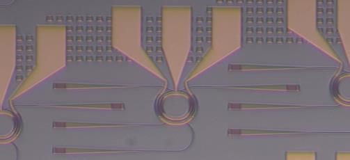
TiN Thermistor
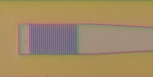
Grating coupling loss 3.8 dB
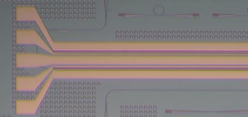
1×2MMI insertion loss 0.043 dB/port
2×2MMI insertion loss 0.27 dB/piece
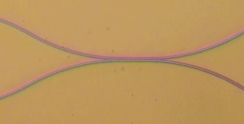
Directional Coupler Custom Splitting Ratio
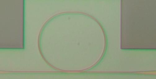
All-pass micro ring Q > 105
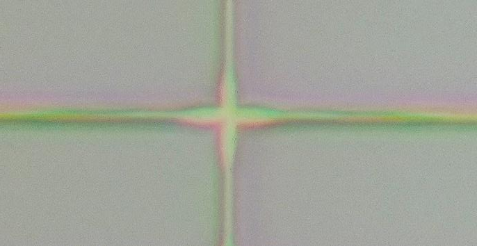
Cross waveguide loss 0.028 dB/piece
Micro-Ring Modulator Bandwidth > 30 GHz
Electro-optical switch extinction ratio 45 dB
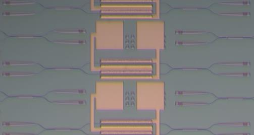
PN Modulator Bandwidth > 30 GHz
OMeda (Shanghai Omedasemi Co.,Ltd) was founded in 2021 by 3 doctors with more than 10 years of experience in nanpfabrication. It currently has 15 employees and has rich experience in nanofabrication (coating, lithography, etching, two-photon printing, bonding) and other processes. We support nanofabrication of 4/6/8-inch wafers.