Business process (must read):
Dear customers, after contacting the sales, please accurately provide the following information to facilitate the technical team to determine whether it can be produced and save communication costs. Please copy the information below and send it to the sales after filling it out. Thank you for your understanding and support.
1. Substrate length, width, thickness and material:
2. Surface film material and thickness (if there is already a film layer on the substrate surface):
3. Film material and thickness of atomic layer substrate:
4. Whether there is structure and glue on the surface, if there is structure, please provide the layout and structure depth, if there is glue, please tell the glue model and thickness:
Capacity description:
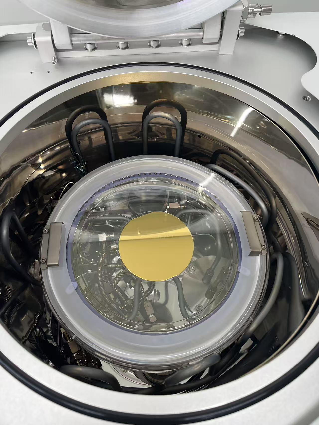
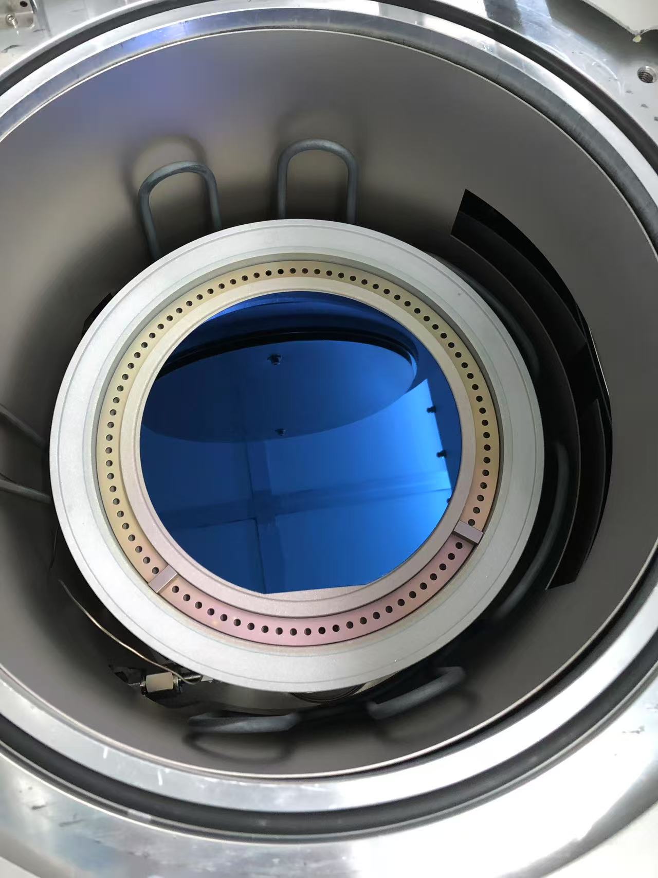
The current equipment configuration is 1 unit 8-inch Benq TFS2000 and the remaining 7 self-made equipment, supporting 2-12 inch atomic layer coating deposition. The sufficient capacity can meet the mass manufacturing and processing needs of corporate customers.
Processing capabilities:
Depositable thin films:
Semiconductor applications:
Oxides: Silicon oxide (SIO2), aluminum oxide (Al2O3), zirconium oxide (ZrO2), hafnium oxide (HfO2), titanium oxide (TiO2), gallium oxide (Ga2O3).
Nitrides: aluminum nitride (AlN), titanium nitride (TiN),
Optical applications: anti-reflection film
Supported size: 2-8 inches (some materials support 12-inch process)
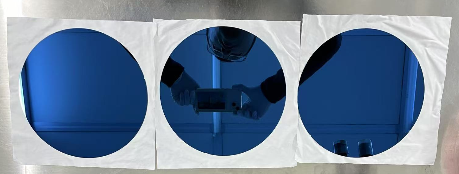
Processing Case:
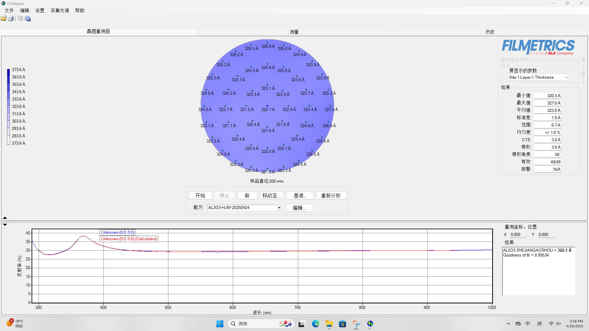
8 inch ALD 30nm Al2O3 (measured film thickness uniformity +-1%)
Equipment:
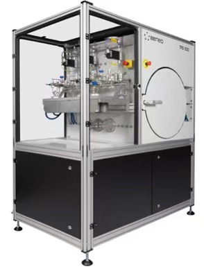
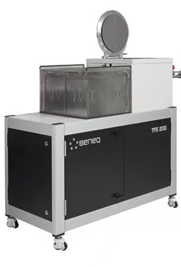
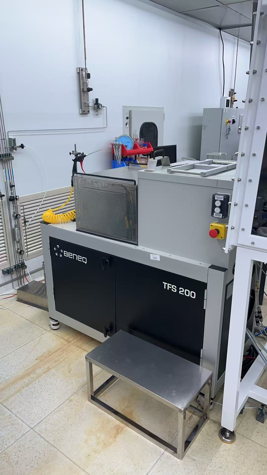
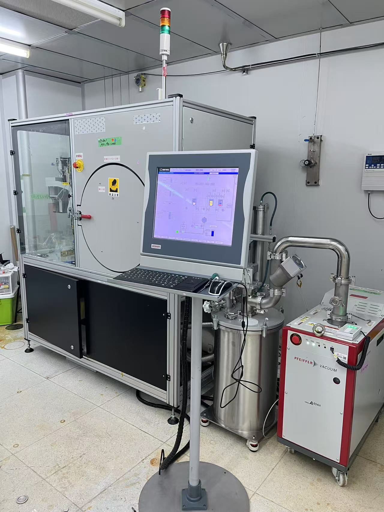
Remarks:
For ALD process, samples must be thoroughly cleaned, temperature-resistant, non-toxic, not easy to decompose, not easy to diffuse (such as Cu), no powder, cannot be marked with a marker, and cannot have high-temperature tape!
Principles:
Atomic layer deposition (ALD) is a thin film deposition technique based on the continuous use of vapor phase chemical processes; it is a subclass of chemical vapor deposition. Most ALD reactions use two chemical species called precursors (also called "reactants"). These precursors react with the material surface one at a time in a continuous, self-limiting manner. Through repeated exposure to separate precursors, thin films are slowly deposited. ALD is a key process for manufacturing semiconductor devices and is part of the toolset for synthesizing nanomaterials.
Advantages:
A--ALD is able to deposit thin films layer by layer, providing excellent control over film thickness. This precision is particularly important in applications such as semiconductors, where nanoscale variations can significantly affect device performance.
B--Conventional deposition techniques have difficulty uniformly coating complex structures, resulting in non-uniform films. Atomic layer deposition overcomes this challenge, ensuring conformal coverage even in complex geometries, making it suitable for microelectronics and microelectromechanical systems (MEMS) devices.
C--ALD's self-limiting reaction makes the film highly uniform, free of defects and thickness variations. This uniformity is critical for applications such as thin-film transistors and protective coatings.
D--Atomic layer deposition is applicable to a wide range of materials, from oxides and nitrides to metals and organic compounds. This versatility allows the creation of novel material combinations and functional structures.
E--ALD's conformal nature extends to high-aspect ratio structures such as nanopores and nanotubes, enabling innovations in energy storage and catalysis.
ALD's controlled process reduces material waste and energy consumption compared to traditional methods, consistent with sustainable manufacturing practices.
Applications:
Gate oxides: ALD addresses the challenge of tunneling current in MOSFETs by depositing high-κ oxides such as Al2O3, ZrO, and HfO22. High-k dielectrics are used as gate insulators to counteract the undesirable effects of quantum tunneling in transistors. This enables thicker gate dielectrics to reduce tunneling current while maintaining the desired capacitance density.
Transition metal nitrides: Atomic layer deposition (ALD) uses transition metal nitrides (e.g., TiN, TaN) to form metal barrier layers and gate metals. These materials wrap around copper interconnects, preventing unwanted diffusion.
Metal films: Atomic layer deposition (ALD) enables copper interconnects, W plugs, and seed layers. It also supports the creation of noble metals for storage capacitors and facilitates the creation of high-work-function and low-work-function metals for dual-gate MOSFETs.
Precision in Magnetic Recording Heads: ALD’s creation of precise insulating layers facilitates magnetic recording heads, enhancing magnetization patterns on hard disks. Precisely controlled insulation thickness improves recording quality.
Shaping DRAM Capacitors: ALD plays a vital role in the fabrication of DRAM capacitors, helping to increase memory density. It helps to extend capacitor functionality while maintaining capacitance levels, which is critical to reducing semiconductor size.
Dielectric Barriers: Atomic Layer Deposition (ALD) creates precise, conformal dielectric barrier layers. These barrier layers are essential for isolating and protecting sensitive components from external contaminants, moisture, and electrical interference.
Passivation Layers: Semiconductor devices often require passivation layers to protect them from environmental factors, prevent corrosion, and ensure long-term functionality. ALD-generated passivation layers provide excellent conformality even on complex and intricate device structures.
Copper Barrier and Seed Layers: Atomic Layer Deposition creates barrier layers for copper interconnects in ICs. These barrier layers prevent copper diffusion into surrounding materials, preventing electrical shorts and improving the overall reliability of interconnect structures. In addition, ALD deposits layers that promote improved adhesion and uniformity during the subsequent copper electrodeposition step.
Packaging and Moisture Barriers: ALD-deposited moisture barrier films provide an effective solution for semiconductor packaging, especially in applications where hermetic sealing is challenging. These films prevent moisture ingress, protecting sensitive components from degradation and extending the life of the device.
MEMS Devices: MEMS require complex structures and precise coatings. ALD provides a method to deposit thin films with atomic-level precision, enabling the creation of powerful and reliable MEMS devices.
3D Integration and Through Silicon Vias (TSVs): ALD facilitates the fabrication of through silicon vias, a key component in three-dimensional integrated circuits (3D ICs). ALD ensures conformal deposition of insulating and barrier layers within TSVs, promoting efficient signal propagation and heat dissipation across vertically stacked layers.
Package-level barrier films: In advanced packaging technologies such as fan-out wafer-level packaging (FOWLP), ALD is used to deposit barrier films to protect sensitive components from moisture, mechanical stress, and external contaminants. These barrier films help improve the reliability and performance of packaged devices.
OMeda (Shanghai Omedasemi Co.,Ltd) was founded in 2021 by 3 doctors with more than 10 years of experience in nanpfabrication. It currently has 15 employees and has rich experience in nanofabrication (coating, lithography, etching, two-photon printing, bonding) and other processes. We support nanofabrication of 4/6/8-inch wafers.