We are glad that you found our Silicon Nitride (Si3N4) optical waveguide processing services on this webpage.
Regarding the processing of silicon nitride optical waveguides, we currently offer two types of services: Electron Beam Lithography and 6-inch DUV direct wafer processing.
The refractive index and absorption data of the silicon nitride thin film wafers we provide:
200nm SIN
 ZJ-200nm-LPCVD+Annealing-SIN.txt
300nm SIN
ZJ-300nm-SINOI -LPCVD+Annealing.txt
400nm SIN
ZJ-400nm-LPCVD+Annealing-SIN.txt
A. Electron Beam Lithography for Optical Waveguides
Advantages: It can achieve waveguide linewidths down to 100nm.
Disadvantages: Only one wafer can be processed per run, which makes it less cost-effective.
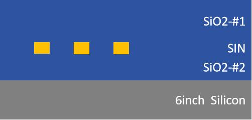
We can process thin films with thicknesses ranging from 100nm to 800nm. We can also deposit SiO2 cladding using two methods: LPCVD and PECVD. Back-end processes include wafer dicing and edge polishing.
Supported Thickness: Up to 800nm.
B. 6-inch 150nm DUV Wafer Processing Line
Advantages: Cost-effective, can process one wafer per run.
Disadvantages: The smallest supported linewidth is currently 150nm.
Current Process Capability: Mature process for 200nm and 400nm Si3N4 thin film thickness wafer processing.
Performance:
Single-end grating loss: around 7.5dB
AWG channel loss, minimum double-end insertion loss: -28dB
Waveguide loss estimation: 0.2~0.5dB/cm
AWG crosstalk: ~20dB
AWG insertion loss: 4dB~5dB
Supported Thickness: Up to 400nm.
Core Specifications:
200nm SiNx Testing:
Waveguide loss estimation: 0.2~0.5dB/cm
AWG crosstalk: ~20dB
AWG insertion loss: 4dB~5dB
Minimum double-end insertion loss: -28dB
Single-end grating loss: around 7.5dB
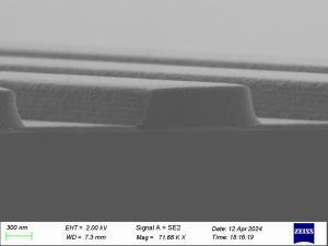
ICP Etching:
ICP SiN etching results
Results for 200nm/400nm
Verticality: >88°
Etching selectivity ratio: around 1.5
6-inch wafer uniformity:<3%
OMeda (Shanghai Omedasemi Co.,Ltd) was founded in 2021 by 3 doctors with more than 10 years of experience in nanpfabrication. It currently has 15 employees and has rich experience in nanofabrication (coating, lithography, etching, two-photon printing, bonding) and other processes. We support nanofabrication of 4/6/8-inch wafers.