When you see this page, if you have limited knowledge of this lithography method, please read this article to choose the processing method that best suits you.
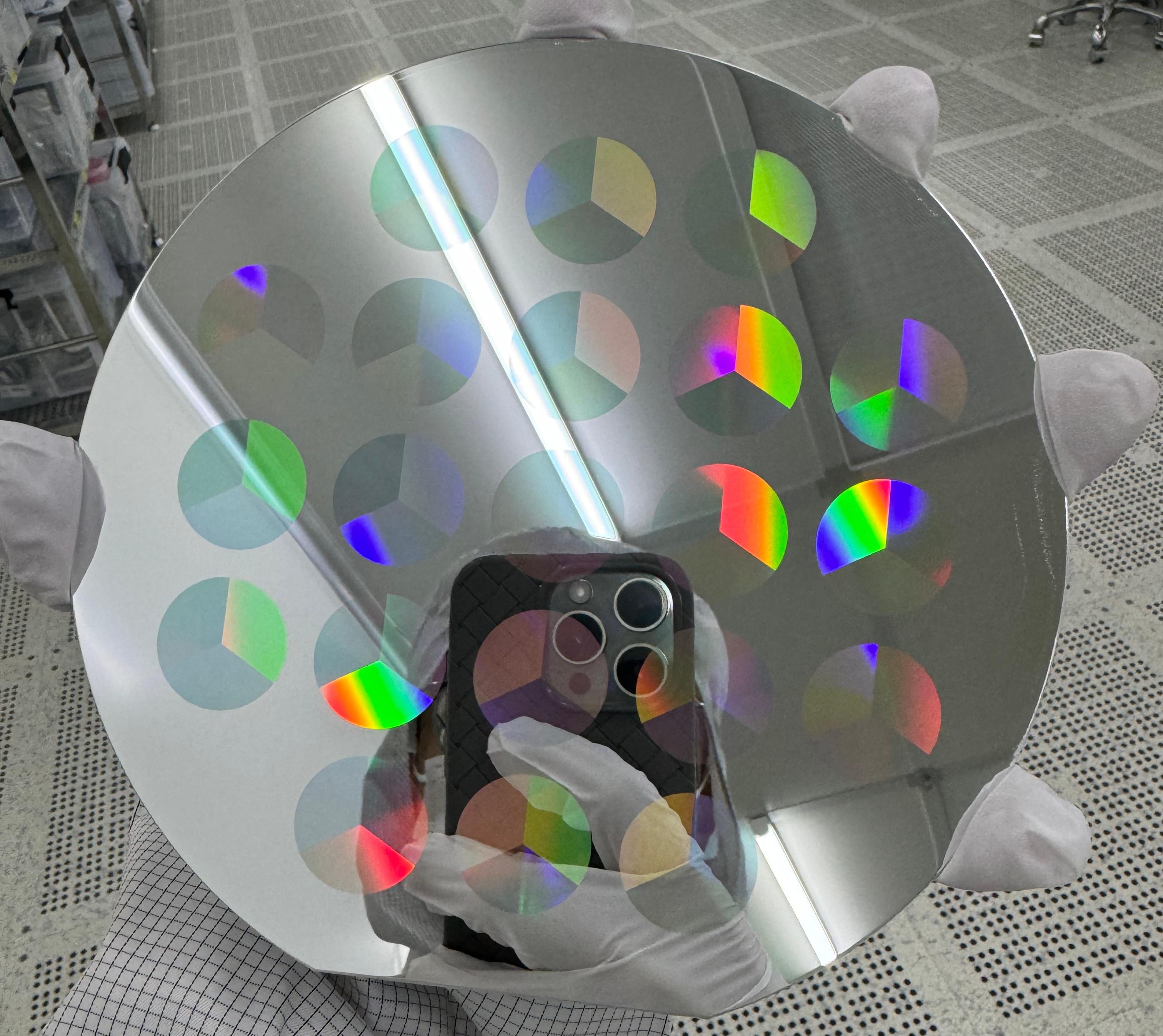
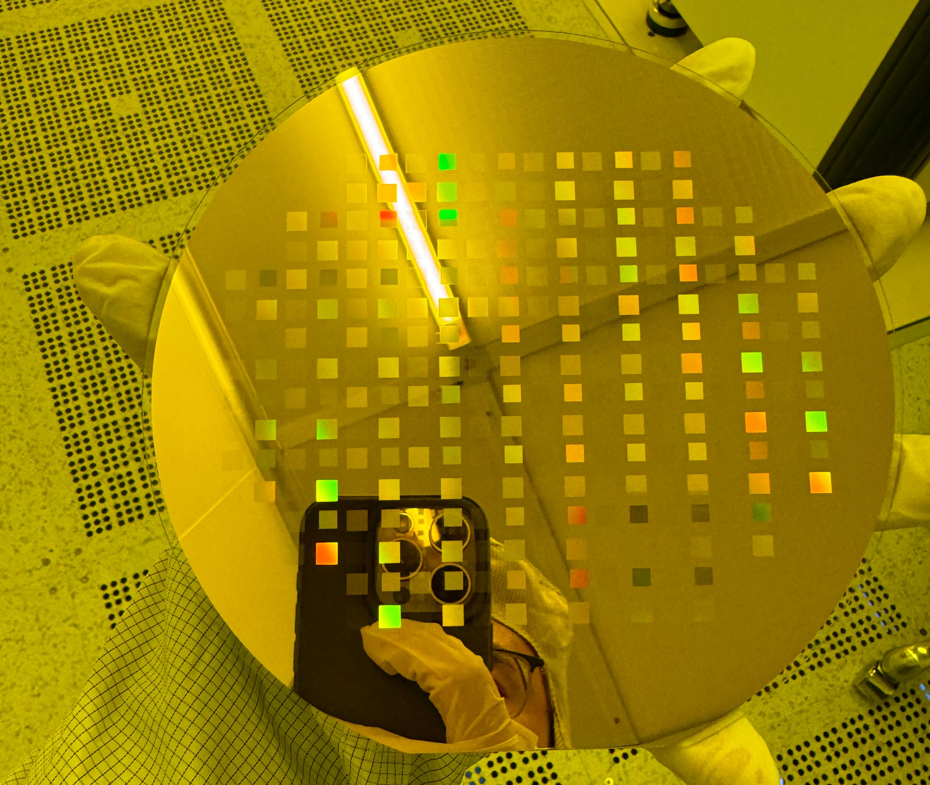
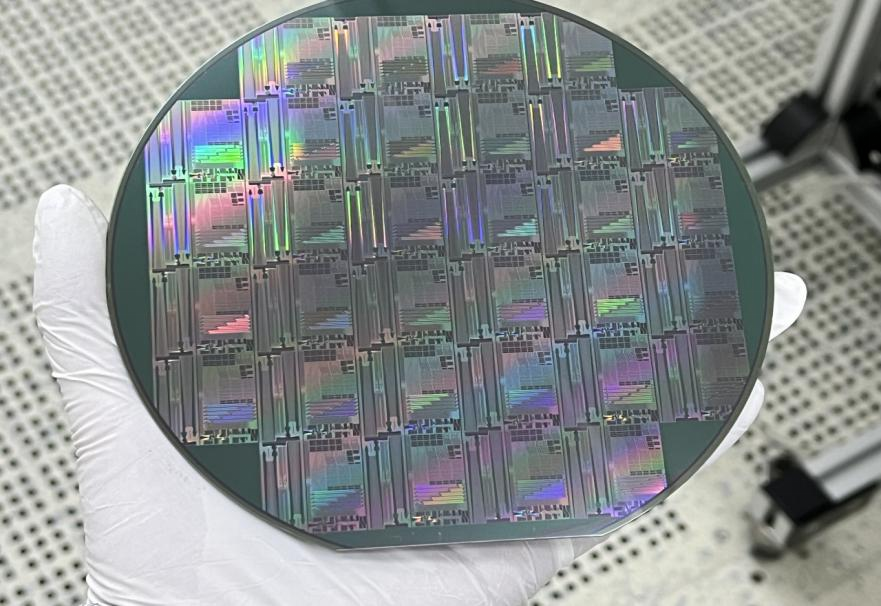
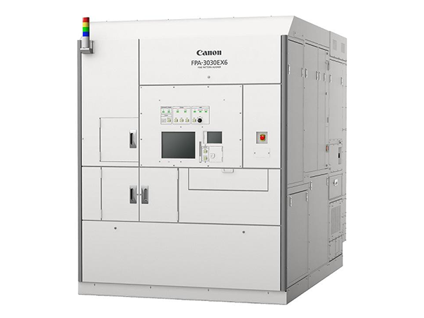
We provide 150nm DUV Stepper lithography service, machine brand and model is Canon FPA-3030EX6, this machine is designed and fabricated by Canon .
its min linewidth is 150nm, and can be used in the high volume production. This equipment has fully automatic spinning, developing and exposing functions and can process 20 pcs 6 inch wafer in one hour. it is an amazing speed and can greatly reduce the cost of lithography and improve the efficiency of lithography .
Application :
Background: Currently, the five mainstream photolithography patterning processes in the semiconductor industry are contact exposure (minimum line width 2µm), laser direct writing (minimum line width 500nm), stepper exposure (Krf minimum line width 150nm, ArF minimum line width 90nm), nanoimprint (minimum line width tens of nm), and electron beam lithography (minimum line width tens of nm).
In the world, there is a high level of equipment availability for electron beam, laser direct writing, contact photolithography, and nanoimprint devices. However, when processing small line widths, electron beam lithography has high costs, low output, and low efficiency. Nanoimprint processing requires obtaining a master template for 1:1 replication, which is also expensive and has a long process flow. Stepper exposure has a certain level of presence domestically, but most DUV systems in research institutes and universities have line widths of 350nm, 450nm, 500nm or higher.
Many industries are rapidly developing, and the AR diffraction optical waveguide, superlens, and photonic integrated circuit industries require more stringent line width specifications. The applications in these markets often require line widths below 250nm.
Therefore, to address the challenges of manufacturing small line width products with low cost, high output, high efficiency, and high precision, solutions are needed.
OMedaSemi offers 6-inch stepper exposure processing with a minimum line width of 150nm, suitable for mass production. The equipment features fully automated spin coating, developing, and exposure functions, capable of processing 20 6-inch wafers per hour. Its speed is remarkable.
Considering the current situation of limited demand and funding from research institutes, universities, and other organizations for such processing, Shanghai OMedaSemi provides two processing modes.
Equipment Introduction:
Substrate Size: 6 inches
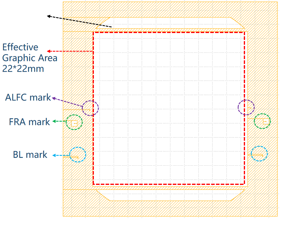
Maximum DIE Size: 22*22mm
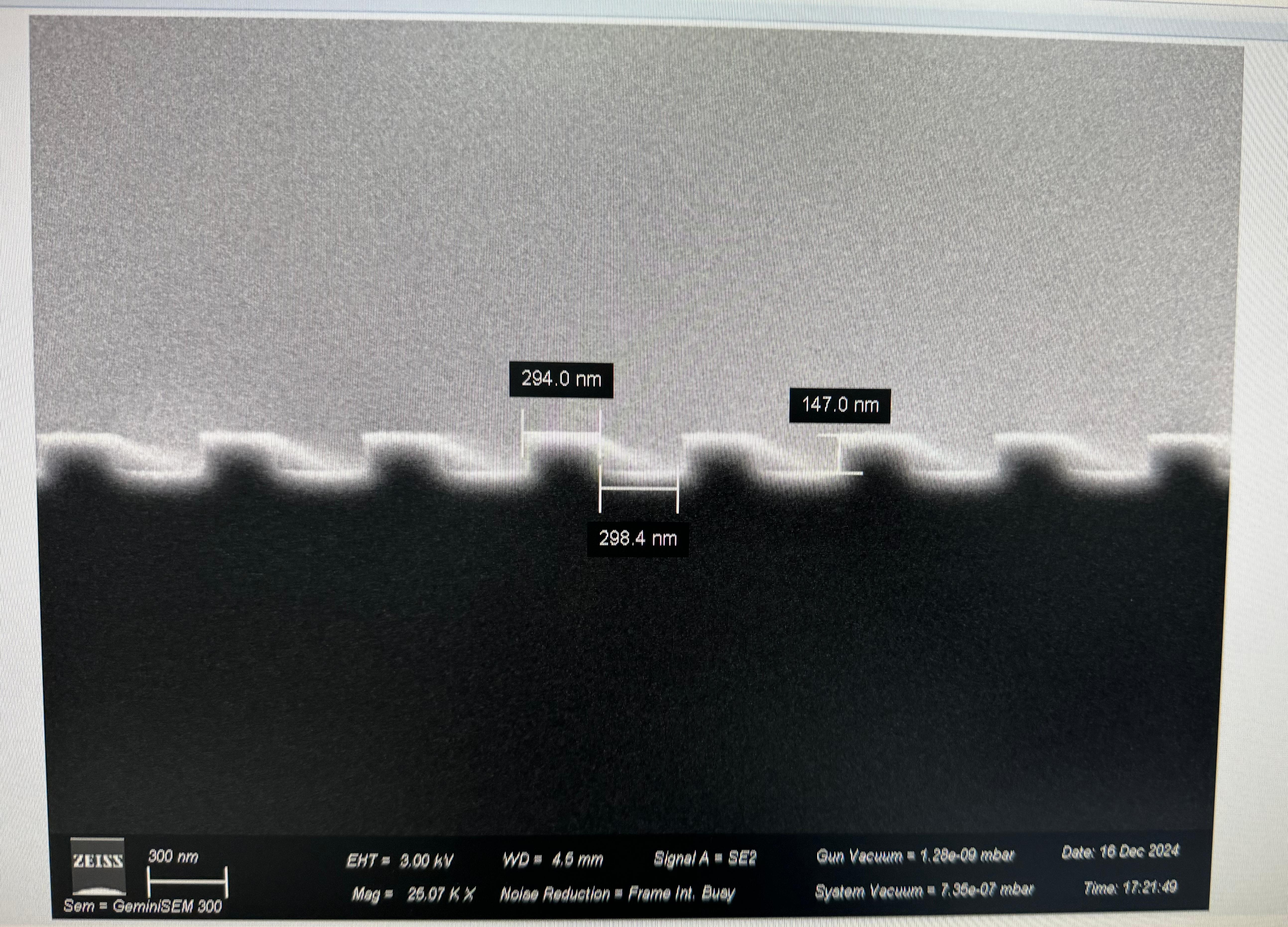
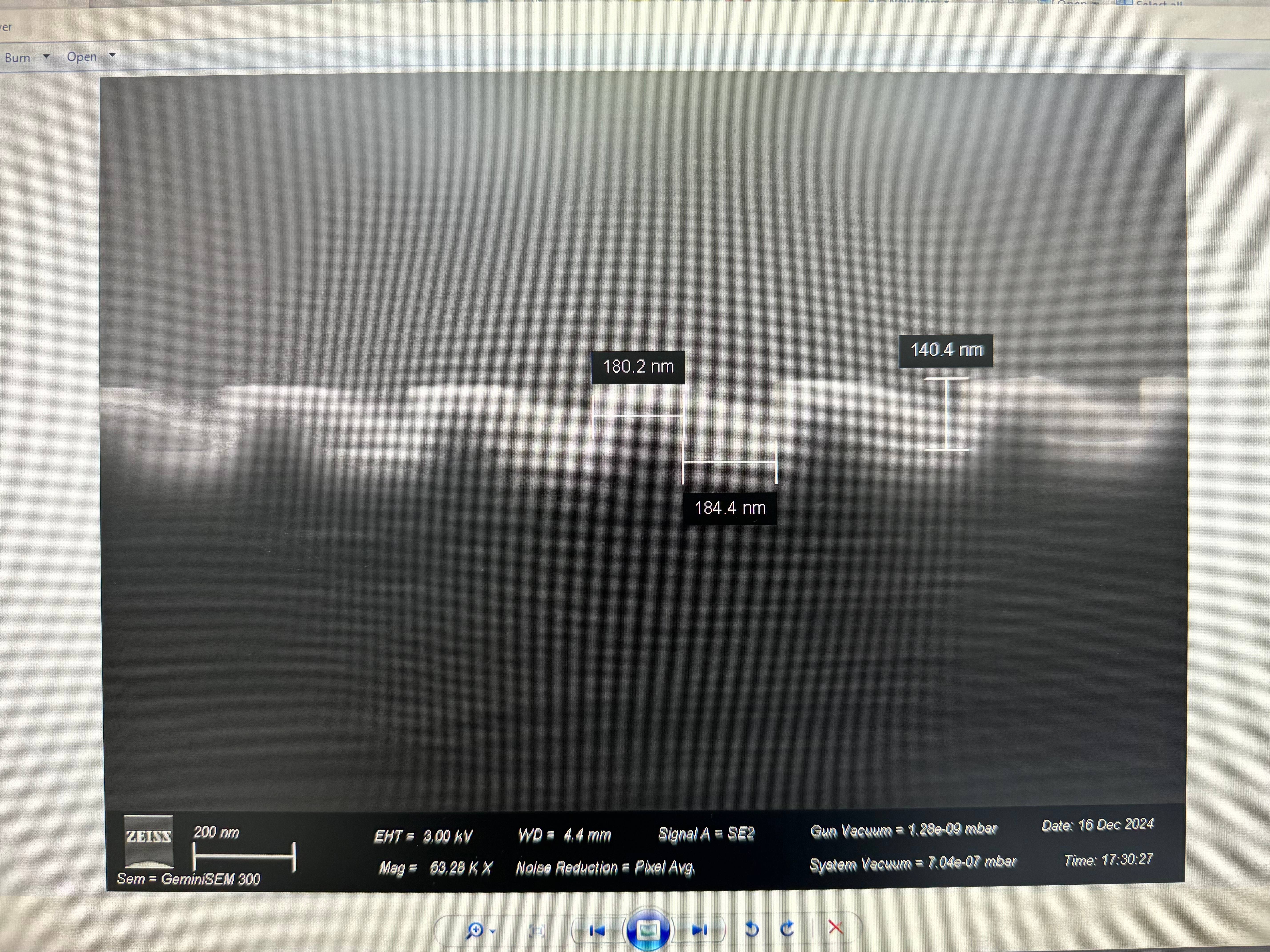
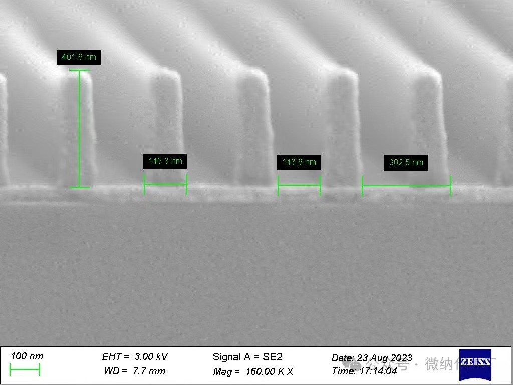
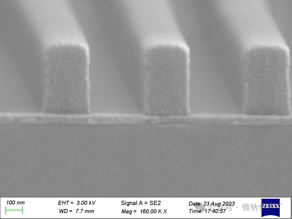
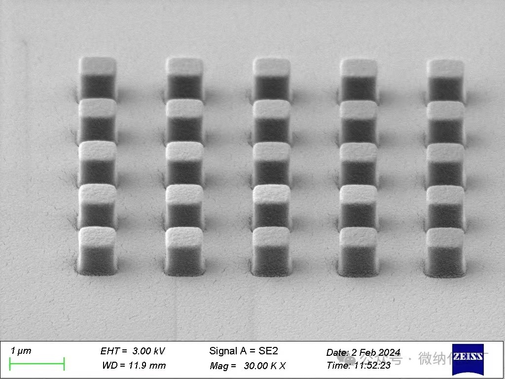
Minimum Line Width: 150 nm
Mask Scaling Ratio: 5 : 1
Alignment Accuracy: ≤40 nm
Focus Accuracy: ≤100 nm
Stepper Accuracy: ≤20 nm
Overlay Accuracy: 30-50 nm
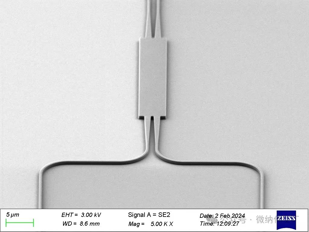
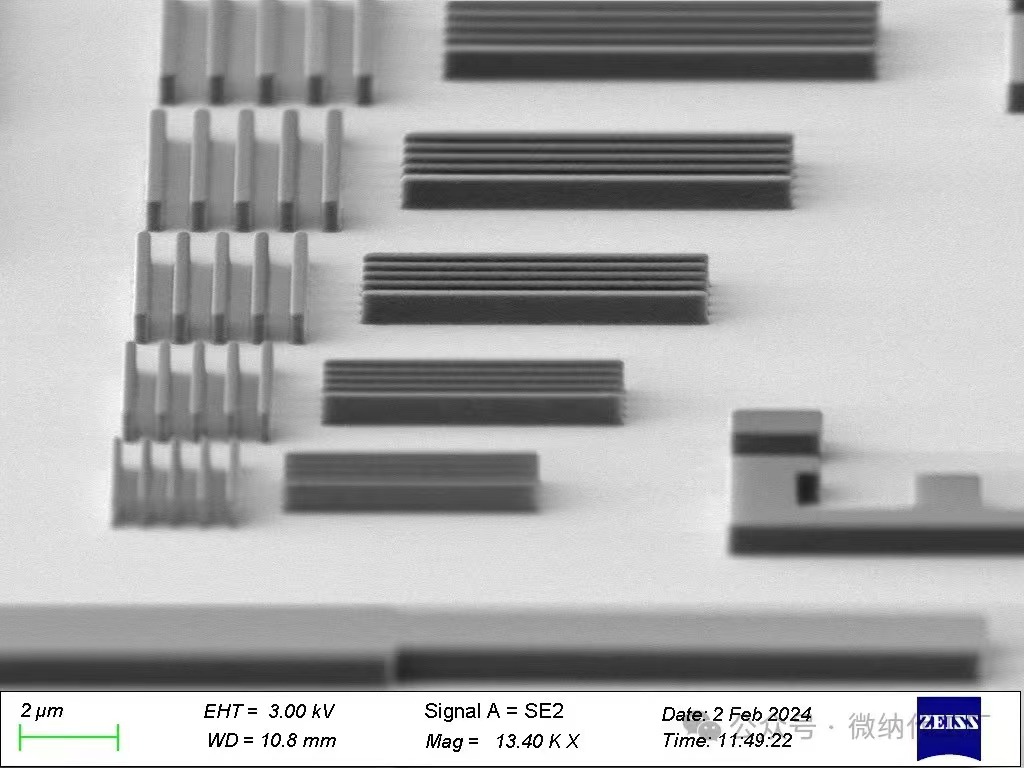
Application Fields: Processing of various micro-nano structures with line widths above 150 nm, diffraction optical waveguides, metastructures, silicon nitride, lithium niobate, silicon photonic waveguides, and other micro-nano structures.
Business Model Introduction
Processing Mode 1: GDS TO DIE (for cases with sufficient budget)
In this mode, we are fully responsible for the entire processing. The customer only needs to provide the layout. After receiving the layout, we conduct a review and confirm the specifications, and then provide the acceptance criteria. We proceed with the full process according to the customer’s requirements, including advance payment, mask making, coating, exposure, development, etching, cutting, packaging, shipping, customer acceptance, and settlement of the balance.
Customer Rights Guarantee: The final delivery will be guaranteed based on the acceptance criteria.
Estimated Cost:
For one 6-inch wafer with a 200nm line width structure, the estimated fee is 10000USD for 1 piece, 12760USD for 2 pieces, and15520 RMB for 3 pieces.
Processing Cycle: 3-4 weeks.
Processing Mode 2: GDS TO Pattern (for limited budget)
In this mode, we only carry out mask making, exposure, and development. The customer will receive the pattern with photoresist. This mode is designed considering:
Most universities already have etching machines to complete the process after exposure.
This mode can save costs.
Customer Rights Guarantee: The final delivery will be guaranteed based on the acceptance criteria.
Estimated Cost:
New Structure - divided into experimental wafer and formal wafer processing:
Processing Cycle: 1 week.
Experimental Wafer Verification:
The customer provides 1 wafer, and we perform FEM (exposure, cutting, SEM, etc.) to determine the precise exposure dose for that film structure. The total etsimated process fee is 1470USD.
Formal Wafer Processing:
Based on the parameters verified from the experimental wafer, we conduct photolithography,the etsimated fee is as following.
3 pieces: 1323 USD
4 pieces: 1764 USD
If there are significant differences from the experimental results, the rework will be done for free.
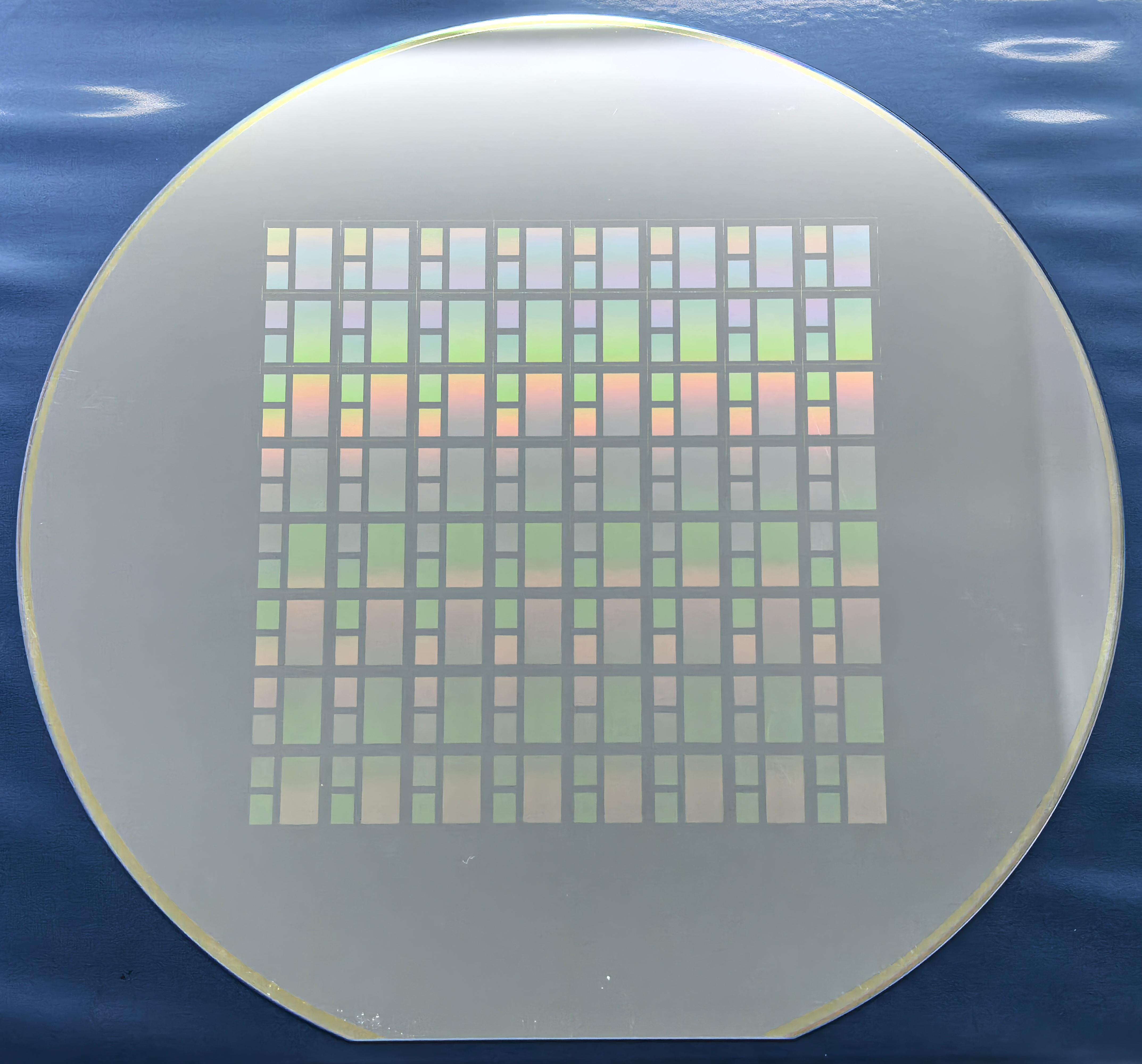
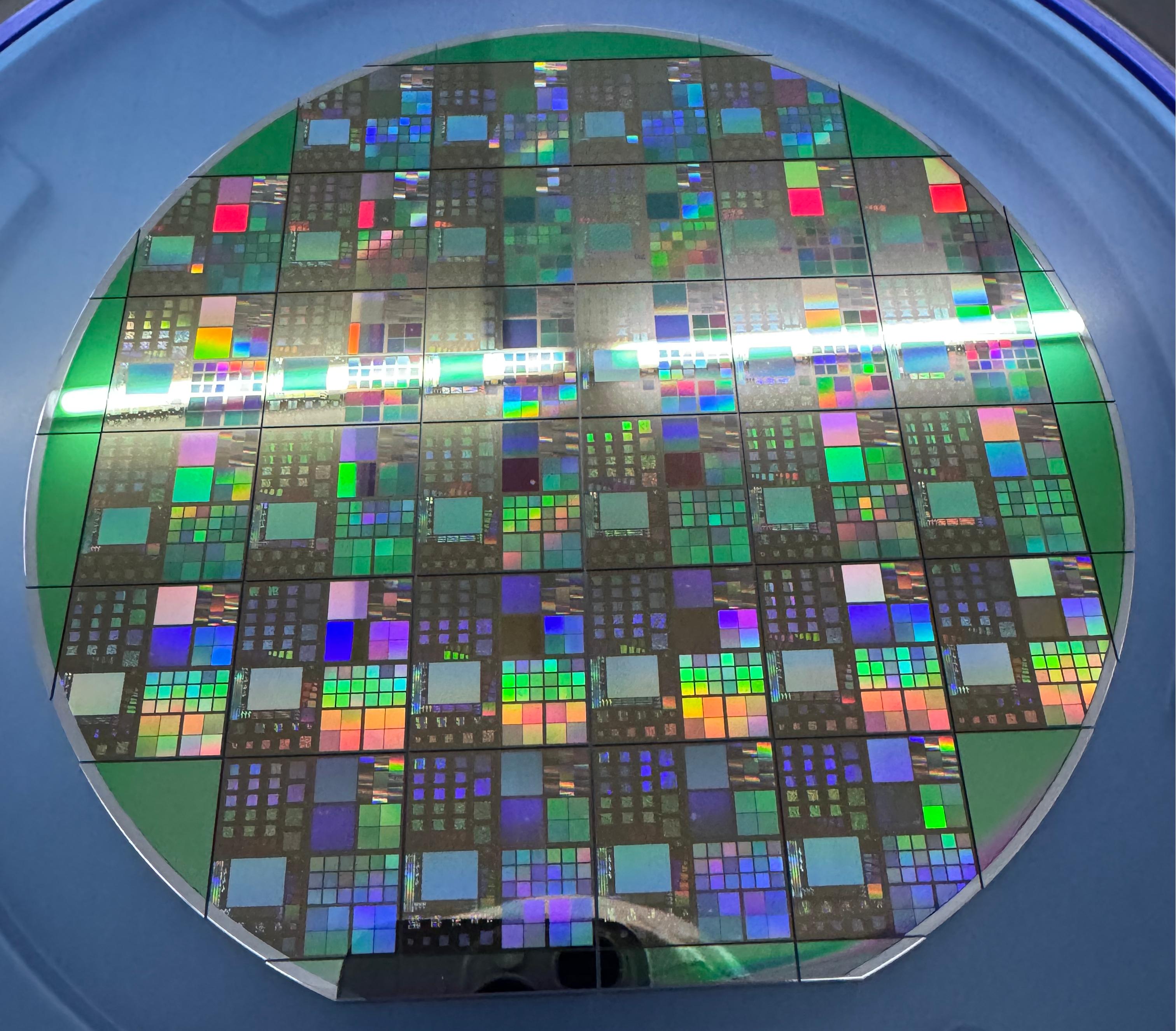
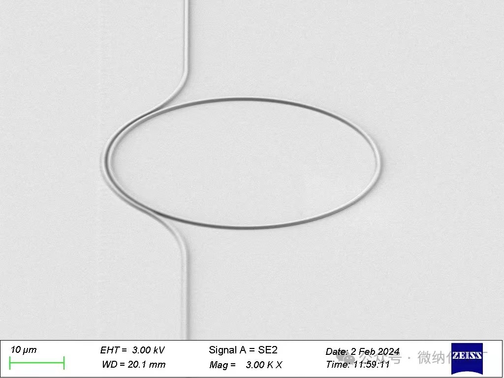
Project that we did
Machine Introduction
No | Item | Description | |
1 | Tool | Lithography machine model | Canon FPA-3030EX6 |
2 | Zoom ratio | 5:01 | |
3 | Exposure light source | 248nm DUV (KrF excimer laser) | |
4 | Mask | SPEC | 6025 |
5 | Material | quartz | |
6 | Size | 6inch(151600 μm to 152400 μm) | |
7 | Thickness | 0.25" (6250 μm to 6450 μm) ) | |
8 | Flatness | Chrome surface within 0.5um | |
9 | Bevel | within 500um | |
10 | Pellicle | SPEC | Select 248nmDUV specification (different from i-line material) |
11 | Frame Inner diameter | 120000(+200,-0)um x 146000(+200,-0)um | |
12 | Frame Outside diameter | 124000(+0,-200)um x 150000(+0,-200)um | |
13 | Frame Width | 2000um | |
14 | Frame Height | 6300±250um |
NOTE:
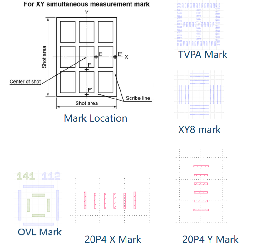
Alignment Mark (essential for overlay): Canon lithography machine alignment mark, including coarse alignment TVPA mark and fine alignment AGA mark;
Each layer that needs to be overlaid requires at least one set of TVPA and AGA marks, and AGA is recommended to be XY8;
Mark positions are as shown in the right figure, placed at the E, E’, F, and F’ positions of the scribe;
Overlay mark is used to measure overlay accuracy, as shown in the right figure, green is the current layer, and blue is the previous layer (it can be omitted if it is not used to measure overlay accuracy)
Marks between different layers should not overlap. (Stepper alignment does not require the mask and wafer marks to be aligned)
The distance between all marks needs to be kept above 250um.
Only one set of the same type of mark is needed for the same layer.
20P4 mark needs to have both Y mark and X mark.
OMeda (Shanghai Omedasemi Co.,Ltd) was founded in 2021 by 3 doctors with more than 10 years of experience in nanpfabrication. It currently has 15 employees and has rich experience in nanofabrication (coating, lithography, etching, two-photon printing, bonding) and other processes. We support nanofabrication of 4/6/8-inch wafers.