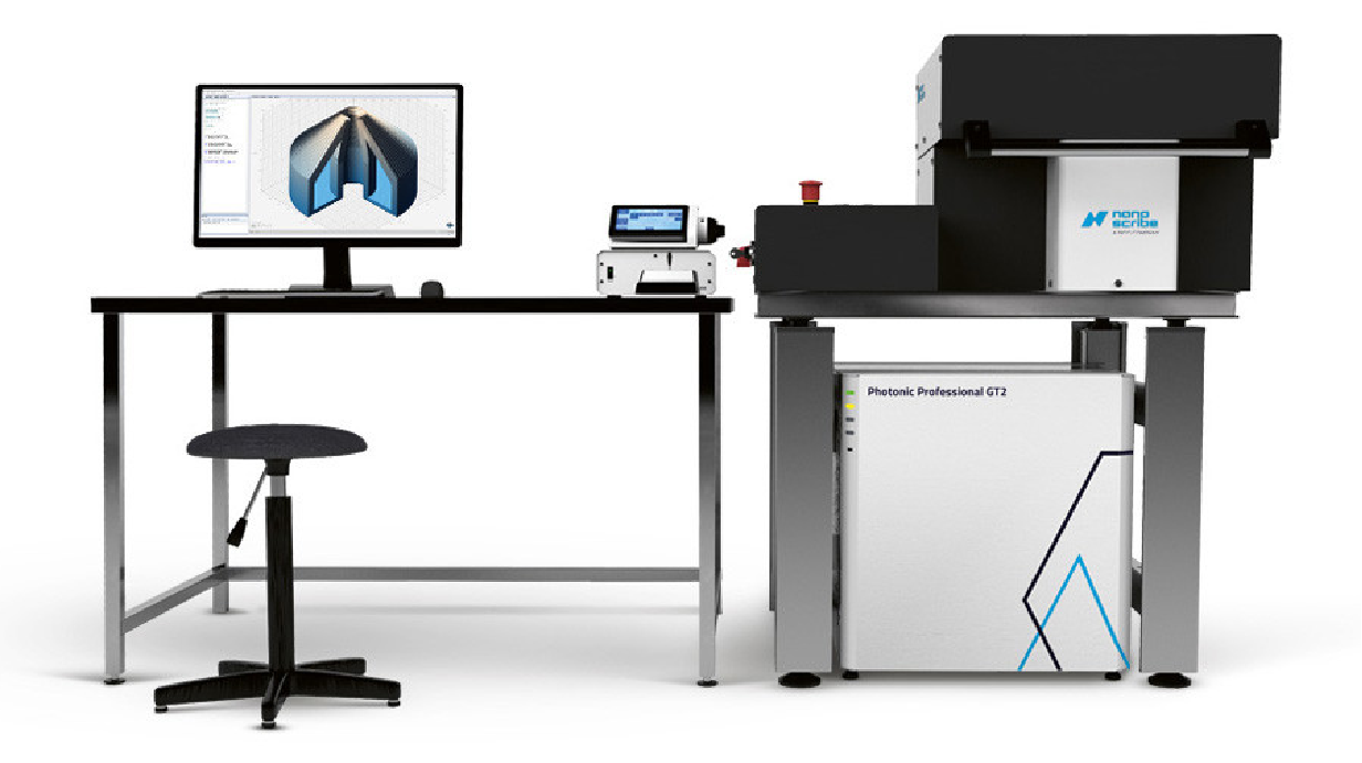
OMedaSemi provide Two Photon 3D Printing Service,we use Nanoscribe Phtonics GT2 Pro & Nanoscribe Quantum X and Nanoscribe IP Dip Glue to print nanostructure on most of substrate .
Processing Capabilities:
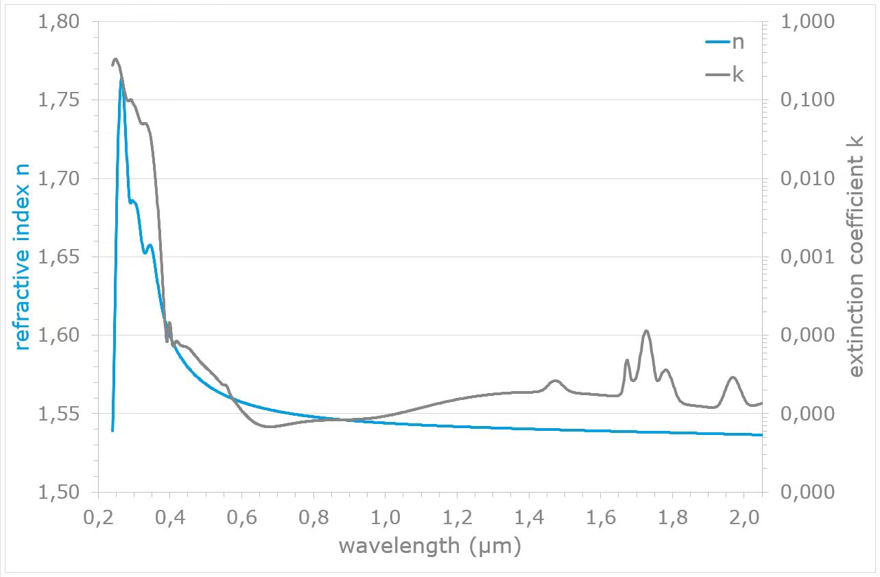
●Refractive index of photoresist: 1.56

Refraction Index of Ip Dip Glue(if you print lens or other optical structure,you can use this data to do simulation),this data is cited from Nanoscribe.com
●Feature size: 200 nm horizontally, 400 nm vertically
●Aspect ratio: 5:1.
●Maximum size: 500um*500um
●Maximum height: 300um
●Substrate: glass/optical fiber/other smooth substrate
●Printing shape: microneedles, microlenses, optical fiber end face structures, diffraction structures, other micro-nano structures
Example that we did:
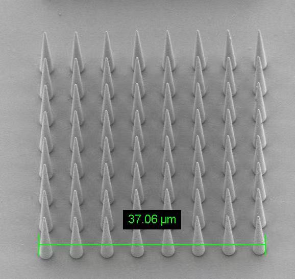
Micro Needle

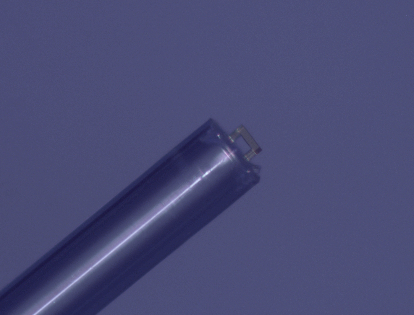
Micro structure on Fiber Tip

Principle:
Two-photon 3D printing (TPP) is an advanced photolithography technology that uses the two-photon absorption effect to form three-dimensional micro-nano structures in photosensitive materials through high-precision laser focusing. The following is a detailed introduction to the basic principles, process flow, application scenarios, advantages and etching accuracy of two-photon 3D printing:
Two-photon 3D printing uses femtosecond laser (usually near-infrared light) to focus on photosensitive materials and trigger polymerization reactions through the two-photon absorption effect:
1. Two-photon absorption: In photosensitive materials, two photons are absorbed by a molecule at the same time, exciting electrons to jump to a higher energy state and trigger chemical reactions.
2. Polymerization reaction: In photosensitive materials, the excited molecules trigger monomer polymerization reactions to form solid polymers.
3. High resolution: Since two-photon absorption only occurs at the laser focus, the energy is concentrated in a very small volume, which can form high-resolution three-dimensional structures.
Equipment introduction:

●Brand: Nanoscribe
●Series: Photonics Pro GT2
●Minimum XY feature size: typical 160 nm; specified 200 nm*
●Most accurate XY resolution: typical 400 nm; specified 500 nm*
●Most accurate vertical resolution: typical 1,000 nm; specified 1,500 nm*
Process flow:
1. Photosensitive material preparation: Select and prepare appropriate photosensitive materials, such as photosensitive resins, and coat or fill them on the substrate.
2. Laser focusing: The femtosecond laser is focused to a specific position inside the photosensitive material through the microscope objective.
3. Pattern design: The three-dimensional motion platform is controlled by a computer, and the laser focus is moved according to the predetermined pattern, and the exposure is scanned layer by layer.
4. Polymerization reaction: The material at the laser focus undergoes polymerization reaction to form a solid structure.
5. Removal of unreacted materials: After the exposure is completed, the unpolymerized photosensitive material is washed away, and only the solidified three-dimensional structure is retained.
Application:
Two-photon 3D printing is widely used in the following fields:
Microelectromechanical systems (MEMS): used to make high-precision microstructures and microdevices.
Biomedical engineering: such as the production of tissue engineering scaffolds, microfluidic chips and bionic structures.
Photonics: such as the production of photonic crystals, optical devices and waveguides.
Materials science: used to study new materials and nanostructures.
Advantages:
Ultra-high resolution: It can achieve submicron or even nanometer resolution, which is suitable for the production of complex micro-nano structures.
Three-dimensional freedom: Ability to focus at any position in three-dimensional space to produce complex three-dimensional structures.
Material diversity: Applicable to a variety of photosensitive materials, including organic and inorganic materials.
Non-contact processing: No physical mask or mold is required, reducing damage and contamination during processing.
OMeda (Shanghai Omedasemi Co.,Ltd) was founded in 2021 by 3 doctors with more than 10 years of experience in nanpfabrication. It currently has 15 employees and has rich experience in nanofabrication (coating, lithography, etching, two-photon printing, bonding) and other processes. We support nanofabrication of 4/6/8-inch wafers.