When you see this page, if you have limited knowledge of this lithography method, please read this article to choose the processing method that best suits you.
We provide customers with electron beam lithography processing services. We have two equipment options: JEOL JBX-9500FS and EUIONIX-ELS-G100. In addition to electron beam lithography, we can also provide a full range of processing services,EBL litho,etching ,dicing. You only need to provide the layout. After receiving the layout, we will conduct project review, quote, and then process according to your needs ,and finish all the fabrication.
Business Process:
#1:Client provide "Substrate information " and "Gds File" amd "fabrication process description"
#2: OMedaSemi will check your drawing and provide feedback about your drawing and fabrication process
#3: After we confirm the drawing and fabrication process ,we will provide "quotation file with the accuracy(the accuracy will be Acceptance Criteria )" that we can promise
#4: If you accept our quotation file ,we can sign the contract ,and then we will arrange the fabrication
#5: Generally ,our fabrication is divided to two part Experimental stage and Formal processing stage :
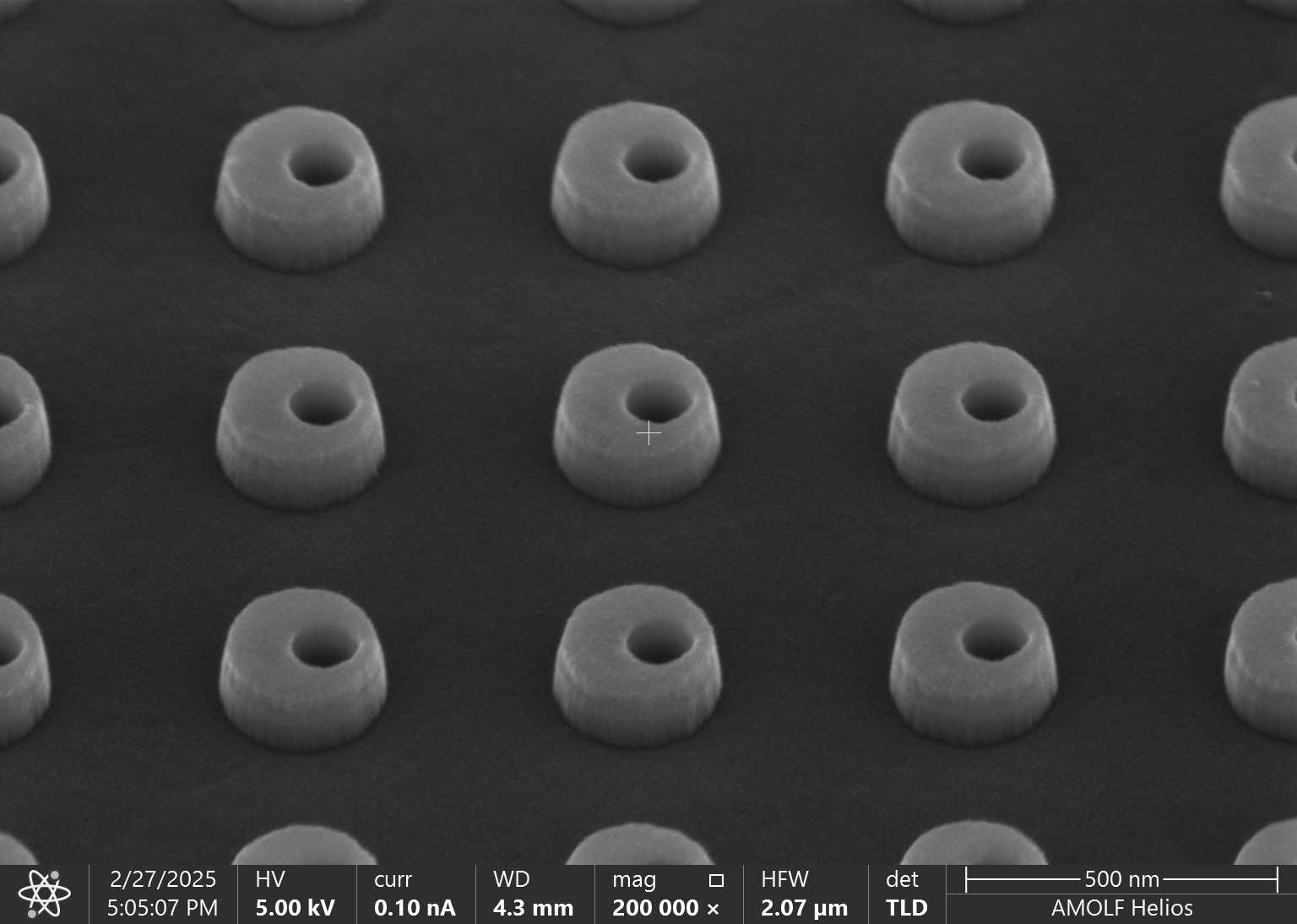
Experimental stage:at first we will choose some area to do the EBL and etching test and then do Fib Sem to Characterize whether it is okay and we get the process parameter of machine by the experiemental stage,the SEM image will be sent to you to confirm whether it can meet your demand .
Formal Processing Stage:We will do formal fabrication according to the parameter ,after we finish the fabrication ,we also provide sem img to you .
#6: After you receive the product and confirm it is okay for you .then you can pay for the fabrication.
#7:Time and Cost—generally lead time is 4 weeks,and because it is EBL litho fabrication process ,so the price is related to Drawing Area , bigger area and more expensive .
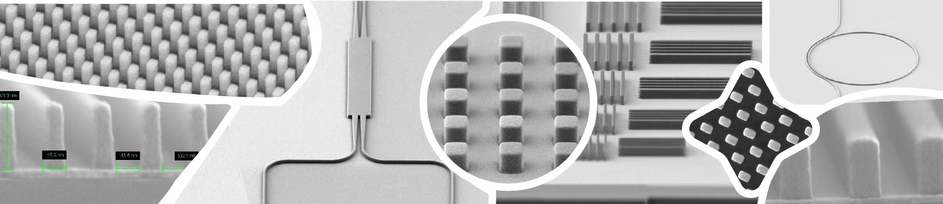
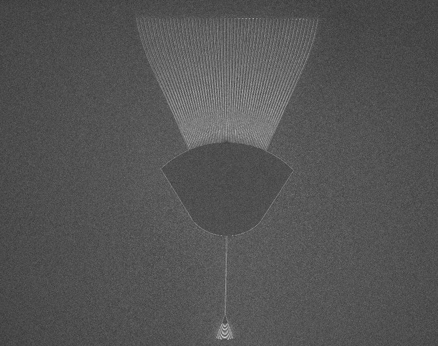
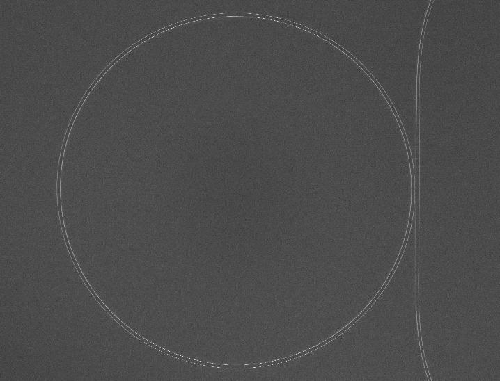
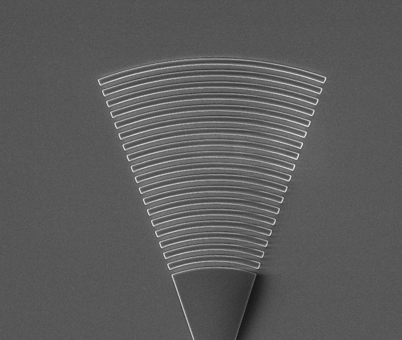
Application: diffraction waveguide/grating, superstructure, silicon nitride/lithium niobate/silicon waveguide, other nanostructures
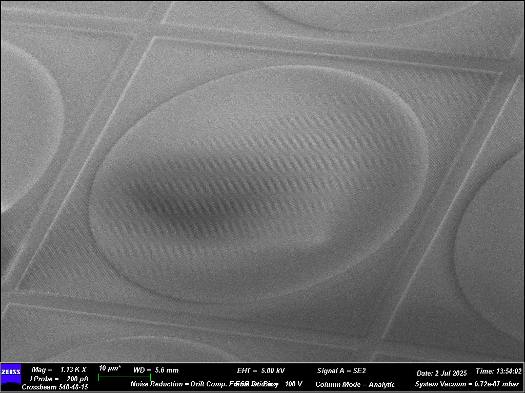
Project Processing--Diffractive waveguide and superstructure
Project Processing--silicon light/lithium niobate/silicon nitride waveguide processing
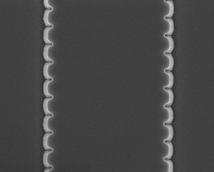
Line Width Accuracy:
>200nm:士5%,
<=200nm: 士10nm
Etching Accuracy:+-10nm
Etching Capabilities:
The electron beam resists we offer are:
Positive resists: ZEP 520, PMMA A4/A10, AR-P 6200
Negative resists: MA-N, HSQ fox14, self-developed thin negative resist
●Application range: AR/VR/PESEL/VCSEL/DFB/
●Material:
Metal: gold/silver/copper/aluminum
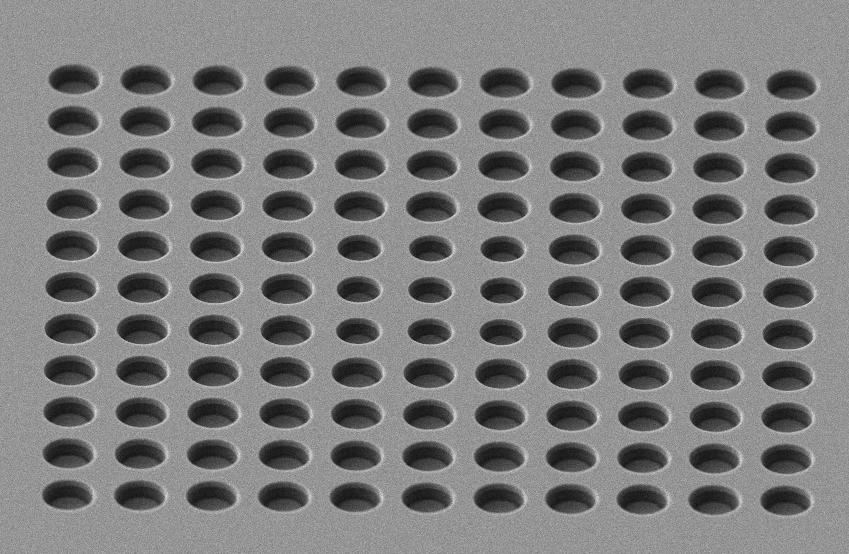
Non-metal: amorphous silicon/Si3N4/SiO2/TiO2/GaN/GaAs/InP
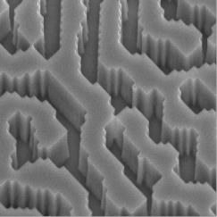
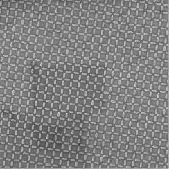
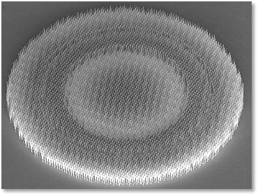
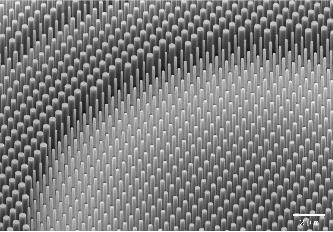
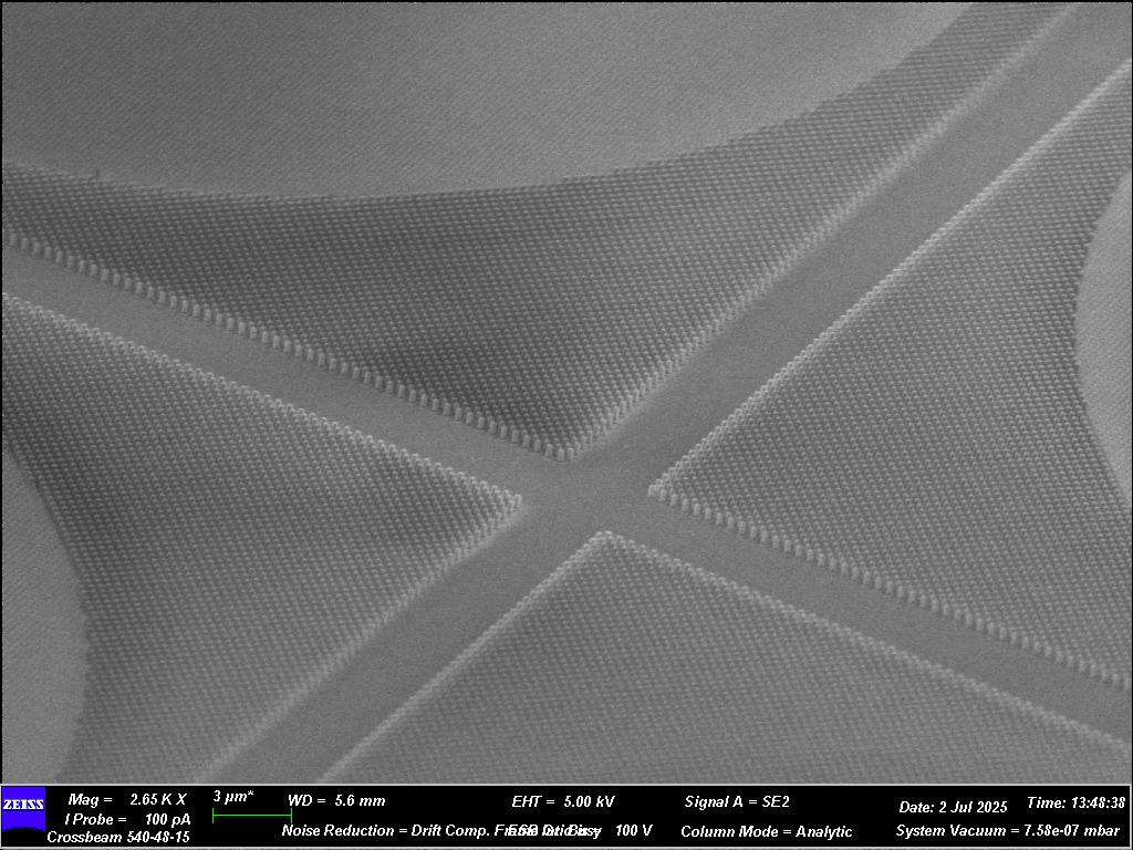
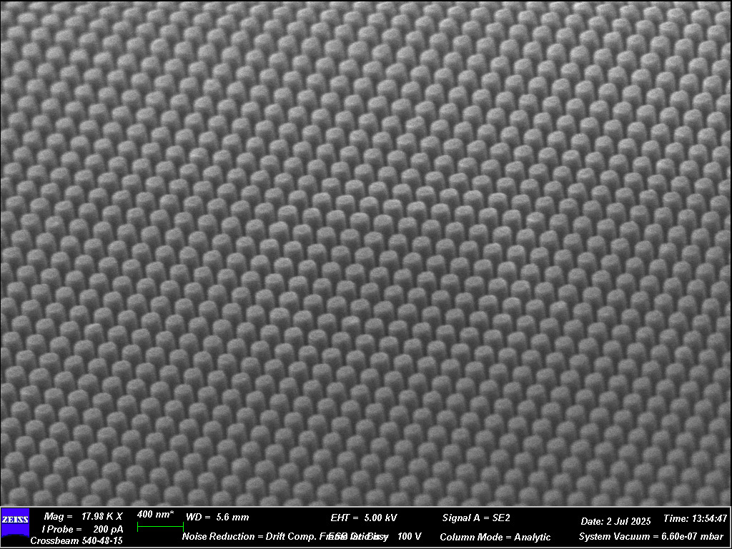
●Type: straight grating/flashing grating/multi-level grating/superstructure/short/circular/triangular and its combination
●Performance:
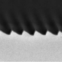
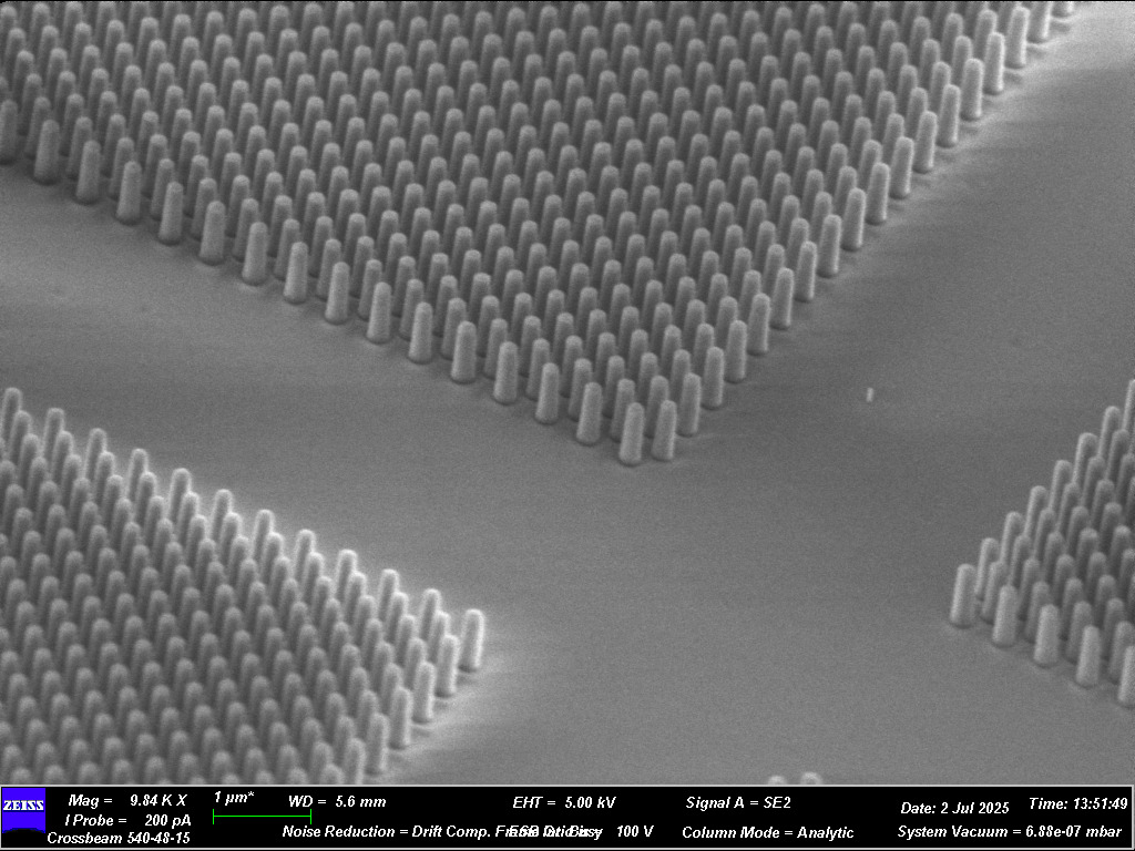
Si feature size 60nm, aspect ratio 10:1, steepness 90±3°
SiO2 feature size 90nm, aspect ratio 4:1, steepness 85±3°
Si3N4 feature size 55nm, aspect ratio 4:1, steepness 85±3°
InP feature size 100nm, aspect ratio 10:1, steepness 85±3°
GaAs feature size 90nm, aspect ratio 10:1, steepness 85±3°
Aluminum Feature size 100nm, aspect ratio 3:1, steepness 85±3°
Gold Feature size 100nm, aspect ratio 3:1, steepness 85±3°
Silver Feature size 100nm, aspect ratio 3:1, steepness 85±3°
Ta2O5
GaN
TiO2 Feature size 100nm, aspect ratio 8:1, steepness 85±3°
Amorphous silicon Feature size 100nm, aspect ratio 10:1, steepness 85±3°
CASE1;Amorphous Silicon Metastructure
Case:
Optics
PIC
Processing Capabilities:
Supported electron beam photoresists: PMMA, HSQ, ZEP
Equipment 1 model: JEOL JBX-9500FS
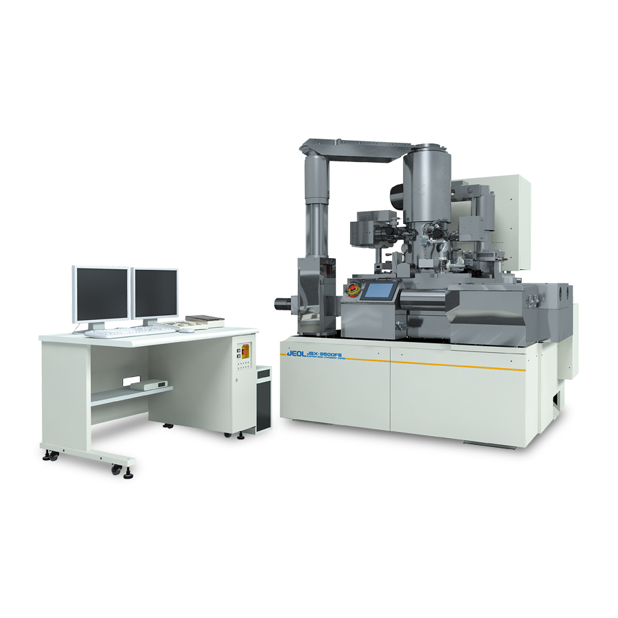
Processing accuracy:
Acceleration voltage: 100KV
Exposure resolution: 10nm
Overlay accuracy: 10nm
Field stitching accuracy: 10nm
Write field size: 1mm*1mm
Scanning frequency: 100MHZ
Acceptable substrate size: 1cm*1cm 2cm*2cm 2 inches 3 inches 4 inches 6 inches
Equipment 2 model: EUIONIX-ELS-G100
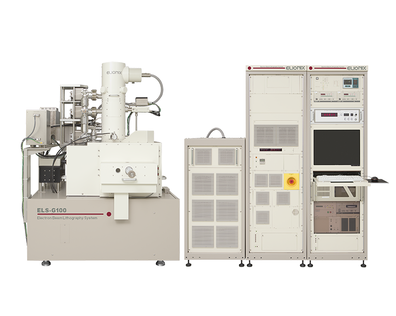
Processing accuracy:
Acceleration voltage: not less than 100 kV
Exposure resolution: 6nm
Overlay accuracy: 20nm
Field stitching accuracy: 15nm
Write field size: 1mm*1mm
Scanning frequency: 100MHZ
Acceptable substrate size: 1cm*1cm 2cm*2cm 2 inches 3 inches 4 inches 6 inches
Principle:
Electron beam lithography (often abbreviated to electron beam lithography or EBL) is the practice of scanning a focused electron beam to draw custom shapes on a surface covered with an electron-sensitive film called a resist (exposure). The electron beam changes the solubility of the resist, selectively removing the exposed or unexposed areas of the resist by immersing it in a solvent (development). As with photolithography, the goal is to create very small structures in the resist, which are subsequently transferred to a substrate material, usually by etching.
The main advantage of electron beam lithography is that it can draw custom patterns with a resolution of less than 10 nm (direct write). This form of maskless lithography has high resolution but low throughput, limiting its use to photomask manufacturing, small-batch production of semiconductor devices, and research and development.
The basic principle of electron beam lithography is to use a high-energy electron beam to write patterns directly on a photosensitive material. The specific steps include:1. Electron beam generation: The electron gun generates a high-energy electron beam, usually using a thermal emission or field emission electron gun. 2. Beam focusing: The electron beam is focused to the nanometer level through the electromagnetic lens system. 3. Beam scanning: The movement of the electron beam is controlled by the scanning coil, and a predetermined pattern is scanned and exposed on the photosensitive material. 4. Photosensitive material reaction: The electron beam interacts with the photoresist (such as positive or negative photoresist) to change the solubility of the photoresist.
Process flow:
1. Substrate preparation: Clean and process the substrate to be etched (such as silicon wafers, glass, etc.), and apply a layer of photoresist.
2. Exposure: In the electron beam lithography system, the desired pattern is formed by controlling the electron beam to scan on the photoresist.
3. Development: Place the exposed photoresist in the developer to dissolve the unexposed (or exposed) area to form a pattern.
4. Etching: Perform an etching process (such as RIE or wet etching) on the developed sample to transfer the pattern to the substrate.
5. Photoresist removal: After etching, remove the remaining photoresist to obtain the final structure.
Application scenarios: Electron beam lithography is widely used in the following fields: Integrated circuit manufacturing: used to make high-precision fine patterns and features. Nanotechnology: such as the production of nanostructures such as nanowires and nanodots. Optoelectronic devices: such as the preparation of optical structures such as waveguides and gratings. Microelectromechanical systems (MEMS): used for precision machining of microstructures. Research and development: suitable for high-resolution research projects and the development of new materials.
Advantages: High resolution: The electron beam has a short wavelength and can achieve sub-nanometer resolution, which is suitable for making extremely small nanostructures. Pattern flexibility: No mask is required, and any complex pattern can be directly written through computer control. High precision: High positioning accuracy, good repeatability, suitable for precision machining.
OMeda (Shanghai Omedasemi Co.,Ltd) was founded in 2021 by 3 doctors with more than 10 years of experience in nanpfabrication. It currently has 15 employees and has rich experience in nanofabrication (coating, lithography, etching, two-photon printing, bonding) and other processes. We support nanofabrication of 4/6/8-inch wafers.