Our company has published an article introducing our PECVD coating capabilities to provide a basic understanding of the PECVD process. For optical applications, we also provide fundamental process parameters and optical testing data to facilitate simulations and evaluations. Furthermore, we have accumulated significant technical expertise in PECVD coating process development and can adjust parameters such as the refractive index and stress of the thin film according to customer needs.
Our company currently mainly provides PECVD coating lines ranging from 2 to 12 inches.
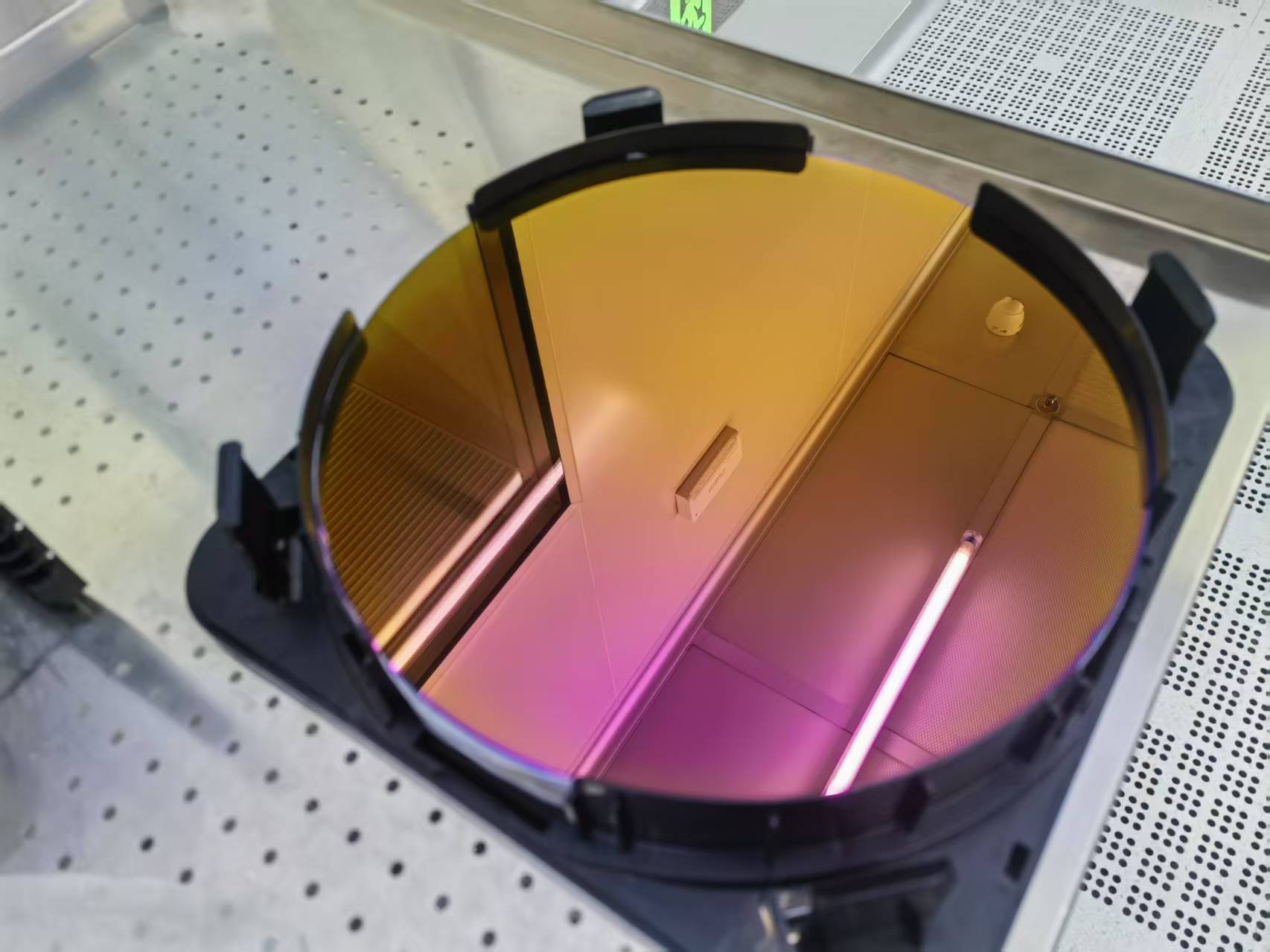
12-inch PECVD Coating Line: --This equipment is primarily used for packaging.
12-inch PECVD Coating (Equipment Name: AMAT PRODUCT GT, 3% film thickness uniformity, 0.5µm particle control<20ea, AOI scan data available):
Supported Materials:
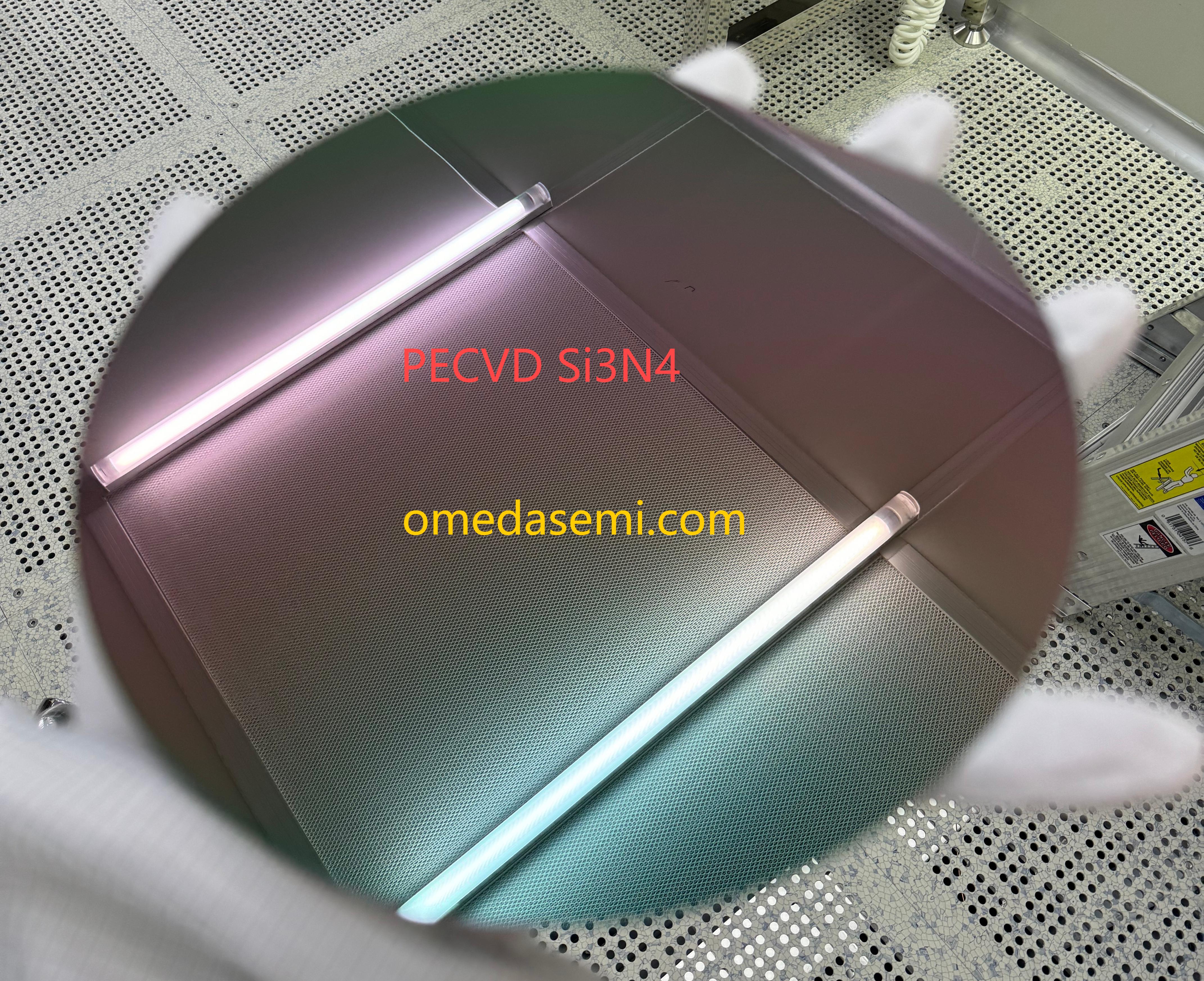
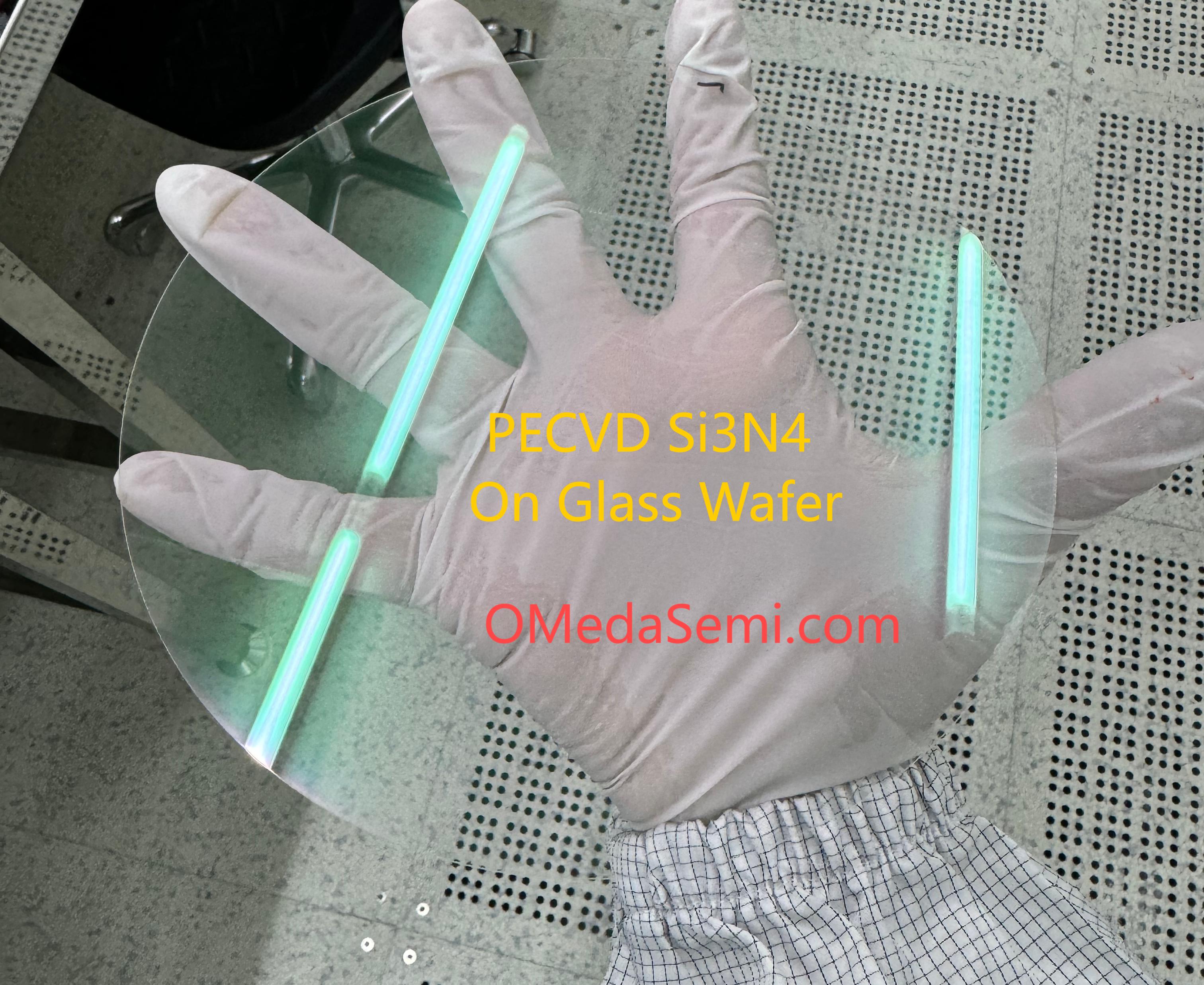
SIN (Process Temperature: 350°C) ,SiO2 (Process Temperature: 180°C-350°C) ,SICN (For state-of-the-art hybrid bonding)
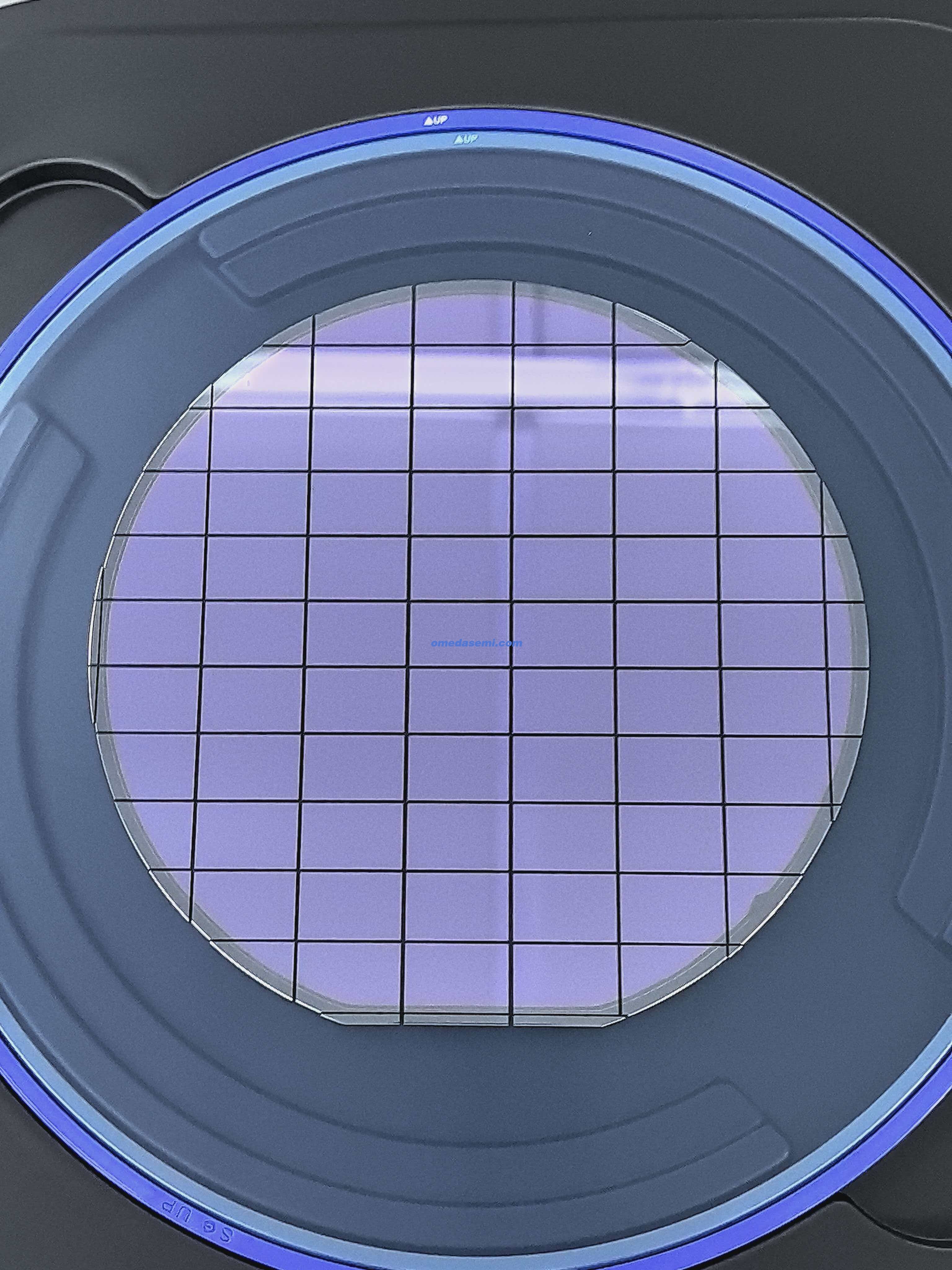
6-inch and 8-inch PECVD Coating Lines
8-inch PECVD Coating (Equipment Name: AMAT PRODUCT GT, 5% film thickness uniformity, no particle control currently available):
Supported Materials:
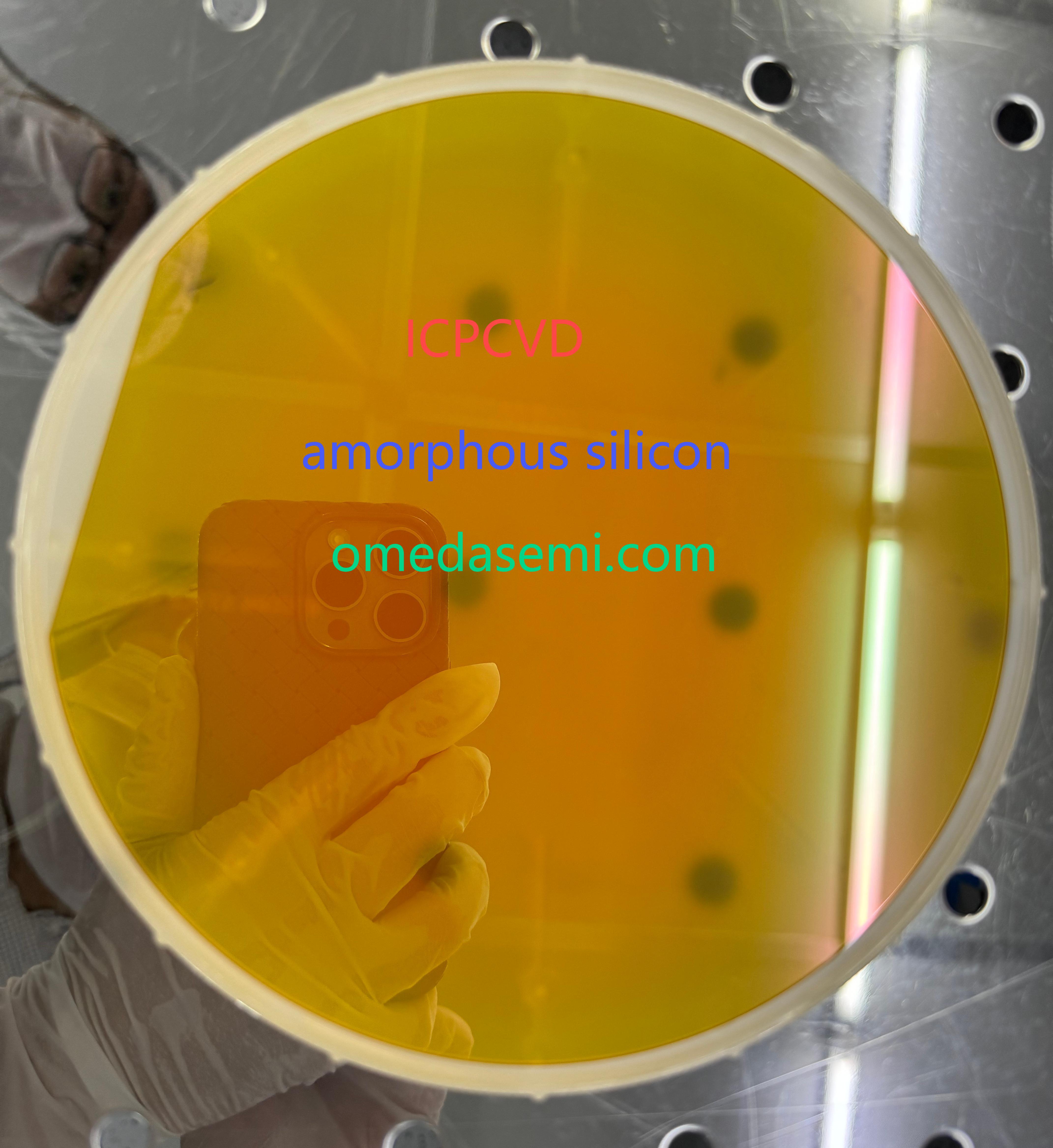
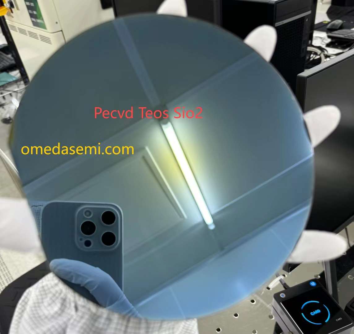
ASI amorphous silicon, SIN (Process Temperature: 350°C), SiO2 (Process Temperature: 350°C), TEOS SIO2
For optical application customers:
Currently, PECVD coating is widely used in optical devices. Amorphous silicon thin films are used for superlenses in the 940-850nm wavelength band, while silicon nitride thin films are used for superlenses and PIC optical devices in the visible light band.
To facilitate your selection, we would like to share the following information:
1. What are the refractive indices of your company's amorphous silicon, silicon nitride, and silicon oxide?
Silicon Oxide:
 PECVD SiO2-200nm on BF33 Schott.docx
Amorphous Silicon:
PECVD a-Si 300nm on Fused Silica JGS1.docx
PECVD a-Si 400nm on Fused Silica JGS1.docx
PECVD 460nm a-Si on Fused Silica JGS1.docx
Silicon Nitride:
 PECVD-SiN-100nm ON 500um 8inch BF33.docx
PECVD-SiN-500nm ON 500um 8inch BF33.docx
PECVD-SiN-50nm ON 500um 8inch BF33.docx
PECVD-SiN-20nm ON 500um 8inch BF33.docx
PECVD-SiN-500nm on Fused Silica.docx
PECVD SiN 1000nm on Fused Silica JGS1.docx
2. What substrate thicknesses do you offer?
Currently, we stock 6-inch JGS1 quartz glass wafers with thicknesses of 500um, 700um, and 800um; 6-inch 675um BF33; 8-inch BF33 glass wafers with a thickness of 725um; and 6-inch and 8-inch 3um hot-melt wafers for PIC device development.
3. Can you dicing wafers?
We have very mature dicing technology.
4. What is the loss rate of your PECVD-deposited silicon nitride?
PECVD, as a 350-degree silicon nitride deposition process, results in relatively high silicon nitride loss due to the presence of hydrogen (H). High-temperature annealing can make the film denser and remove the H.
However, PECVD silicon nitride is relatively inexpensive and easy to obtain, making it a low-cost and efficient method for process verification. If your budget is limited, trying it out might be a good option.
Business Process (Required Reading):
Dear Customer, after contacting sales, please provide the following information accurately to help the technical team determine if production is feasible and save communication costs. Please copy the information below, fill it out, and send it to sales. Thank you for your understanding and support.
1. Substrate length, width, thickness, and material:
2. Surface film material and thickness (if the substrate surface already has a film):
3. Film material and thickness of the substrate requiring atomic layer deposition:
4. Whether there is a surface structure and adhesive. If there is a structure, please provide the layout and structure depth. If there is adhesive, please specify the adhesive type and thickness:
Know more about our Coating Capbility
| Material | EBE | magnetron Sputtering | IBS | PECVD | ICPCVD | LPCVD | ALD | PLD | MOCVD | MBE |
| Au | O | O | ||||||||
| Ag | O | O | ||||||||
| Ta | O | |||||||||
| Al | O | O | ||||||||
| Cu | O | |||||||||
| Fe | O | |||||||||
| Mo | O | |||||||||
| Ti | O | O | ||||||||
| Ni | O | O | ||||||||
| W | O | |||||||||
| Ge | O | |||||||||
| Ir | O | |||||||||
| Zr | O | |||||||||
| Pt | O | O | ||||||||
| Cr | O | O | ||||||||
| NiCr | O | |||||||||
| TiW | O | |||||||||
| WC | O | |||||||||
| C | O | |||||||||
| NiSn | O | |||||||||
| AgSn | O | |||||||||
| AuSn | O | O | ||||||||
| MoS2 | O | |||||||||
| Ta2O5 | O | O | ||||||||
| TiO2 | O | O | O | |||||||
| GaO | O | |||||||||
| Ga2O3 | O | |||||||||
| Al2O3 | O | O | ||||||||
| IZO | O | |||||||||
| IGZO | O | |||||||||
| ITO | O | |||||||||
| CeO | O | |||||||||
| HfO2 | O | O | ||||||||
| NiO | O | |||||||||
| ZrO2 | O | O | O | |||||||
| Y2O3 | O | |||||||||
| WO3 | O | |||||||||
| MgO | O | O | O | |||||||
| GaN | O | |||||||||
| AlScN | O | |||||||||
| AlN | O | |||||||||
| TiN | O | |||||||||
| SiNX | O | O | ||||||||
| Si3N4 | O | O | O | |||||||
| SiC | O | |||||||||
| SiON | O | |||||||||
| Poly Si | O | |||||||||
| α Si | O | O | O | |||||||
| TEOS Sio2 | O | O | ||||||||
| SrTiO3 | O | |||||||||
| BaTiO3 | O | |||||||||
| MgF2 | O |
OMeda (Shanghai Omedasemi Co.,Ltd) was founded in 2021 by 3 doctors with more than 10 years of experience in nanpfabrication. It currently has 15 employees and has rich experience in nanofabrication (coating, lithography, etching, two-photon printing, bonding) and other processes. We support nanofabrication of 4/6/8-inch wafers.