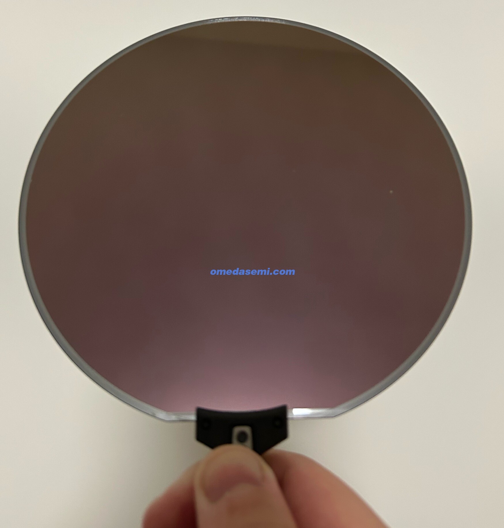
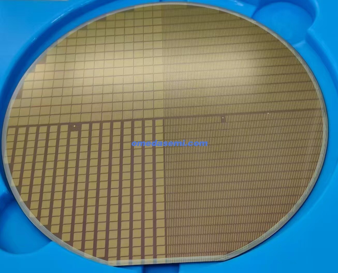
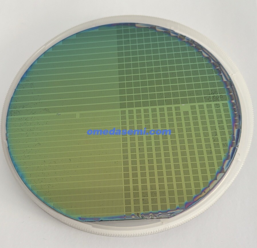
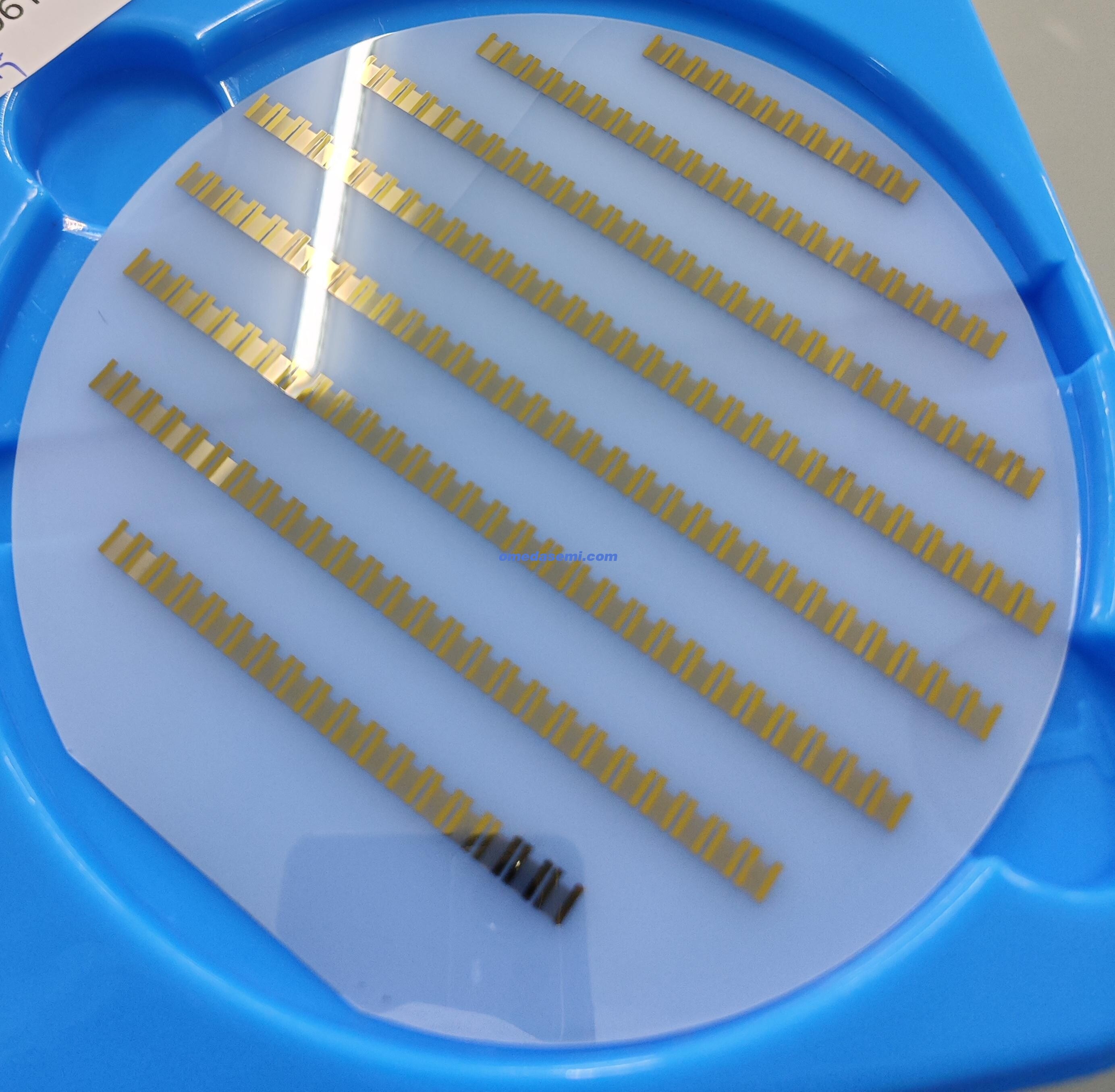
OMedaSemi provides acoustic device processing services, combining photolithography, stripping, coating, deep silicon etching, and dicing to offer a wide range of processing services. We also possess a 6-inch DUV 150nm photolithography system, capable of processing high-frequency acoustic devices. We also offer bonding, ion implantation, thinning, and polishing processes, enabling us to fabricate a variety of acoustic composite substrates. We offer a comprehensive process flow from design, substrate fabrication, processing, and dicing.
Applications:
BAW Devices
SAW Devices
FBAR Devices
TC SAW Devices
Processing Types:
IDT Electrode Fabrication
Backside Deep Silicon Etching Cavity Opening
Mo PVD Deposition
AlScN Deposition (0-20Sc%)
Case 1: Double-layer LNOI Wafer - Front-side Electrode Fabrication - Backside Deep Silicon Etching
Substrate - Front-side Metal Electrode - Backside Deep Silicon Etching


Case 2: Interdigital electrodes (interdigital transducers) on the surface of lithium niobate crystals

OMeda (Shanghai Omedasemi Co.,Ltd) was founded in 2021 by 3 doctors with more than 10 years of experience in nanpfabrication. It currently has 15 employees and has rich experience in nanofabrication (coating, lithography, etching, two-photon printing, bonding) and other processes. We support nanofabrication of 4/6/8-inch wafers.

