We provide 4-8 inch LTOI wafers (thin film lithium tantalate),We can provide 4inch 6inch 8inch lithium tantalate on insulator wafer , Both thin film (300-600nm) by smartcut process and Thick Film (>600nm) by Grinding+CMP process

Optical Data we provide:Refractive Index and Absorption Data For Photonics integrated Circuit
Related Paper About LTOI Application (if you are not familiar with this material,please see the following paper first
Arrayed waveguide gratings in lithium tantalate integrated photonics.pdf
 Robust Poling and Frequency Conversion on Thin-Film Periodically Poled Lithium.pdf
A sub-volt near-IR lithium tantalate electro-optic modulator.pdf
Efficient and tunable frequency conversion using periodically poled thin-film lithium.pdf
Low-loss_lithium_tantalate_on_insulator_waveguide_towards_on-chip_nonlinear_photonics.pdf
Copper Damascene Process-Based High-Performance Thin Film Lithium Tantalate Modulators.pdf
Periodic poling of thin-film lithium tantalate by.pdf
Lithium tantalate microring cavities with Q factor exceeding 10 million.pdf
Our Innovation:
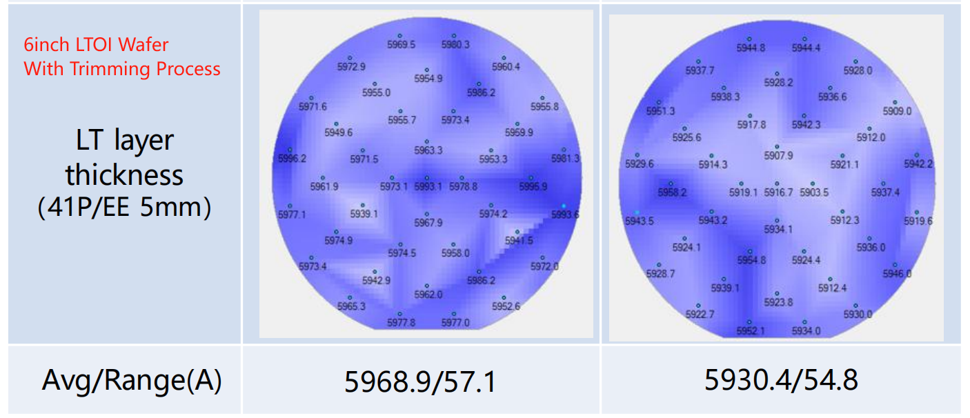
Compared with general LNOI wafer ,we add a innovative process:"Gas Cluster Ion Beam Trimming process " to improve the uniformity(Thickness uniformity Range<57A) of LN thickness and get lower roughness .
6 inch LTOI Wafer Without Trimming Service: Range 100A-200A

6 inch LTOI Wafer With Trimming Process:Range:<57A
Please click to know more about the " Gas Cluster Ion Beam Trimming Process"
Application:
SAW surface acoustic wave device--POI wafer
TFLT PIC thin film lithium tantalate photonic integrated circuit
Supported size: 4 inch 6 inch 8inch
Crystal cut: X cut (optical), Y cut-Y42 (SAW), Z cut (quantum)
Lithium Tantalate layer thickness: 300nm-600nm (SMARTCUT), >600nm (thinning and polishing)
Thermal oxide layer thickness: 50nm-20um
Substrate thickness: 4 inches (675um), 6 inches (675um), 8 inches (725um)
Processing technology: hydrophilic bonding + annealing, surface activation bonding
Customized processing: In addition to standard LTOI wafers, we also provide customized processing services for LTOI wafers.
Our advantages: Full process, comprehensive processing capabilities
*Ion implantation*Thinning and polishing*Surface activation bonding*Hydrophilic bonding*Annealing*Ultra-high precision TRIM polishing Comprehensive processing capabilities can provide you with fast, efficient and customized processing services.
Data Support:
Refractive index and Absorption of Bulk crystal and Thin Film Crystal.zip
Lithium tantalate thin films are divided into thick films (greater than 600nm) and thin films (300nm-600nm)
Thin film lithium tantalate(300nm-600nm)
Using hydrophilic bonding or surface activation bonding technology, the lithium tantalate crystal is first ion implanted, and then the thermal oxide sheet and the X-cut or Z-cut lithium tantalate crystal wafer are bonded together. The defects of ion implantation are enlarged by annealing, and the lithium tantalate substrate is peeled off, leaving the lithium tantalate thin film. The surface is CMP polished and ion beam refined to obtain the finished product, and the thickness is controlled to the thickness you need.
Thick film lithium tantalate(>600nm for quantum application )
Using hydrophilic bonding or surface activated bonding technology, the lithium tantalate crystal and the thermal oxide sheet are directly bonded together, and then the lithium tantalate crystal is directly thinned by thinning and polishing to a thickness of about 10um, and then CMP processing is performed. After polishing to an approximate thickness, ion beam finishing is performed to fine-tune the film thickness accuracy of the surface. The resulting wafer can maintain a film thickness uniformity of +-100nm on a 6-inch wafer.
It is worth noting that ion implantation and direct CMP and thinning have their own advantages and disadvantages. We provide customers with a variety of LNOI products.
Lithium tantalate crystals are divided into Congrudent Lithium Tantalate and Near-Stoichiometric lithium tantalate
We can also provide near-stoichiometric lithium tantalate. Compared with the isocratic lithium tantalate crystals commonly used in the market, near-stoichiometric lithium tantalate crystals have larger electro-optic coefficients and nonlinear optical coefficients, as well as smaller coercive fields and smaller short-wave absorption. It can show better performance. At present, the same composition thin film lithium tantalate wafer supports 4-8 inch processing, and the near stoichiometric thin film lithium tantalate wafer supports 4-6 inch processing. If you are interested in near stoichiometric lithium tantalate, please click this link: Near stoichiometric lithium tantalate (NSLT) wafers
Related Paper
Copper Damascene Process-Based High-Performance Thin Film Lithium Tantalate Modulators.pdf
Overal Test Data (X cut 600nm LT-4700nm SIO2-675um SI )
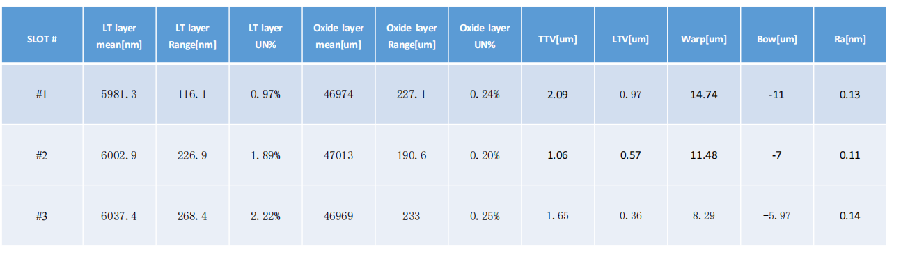
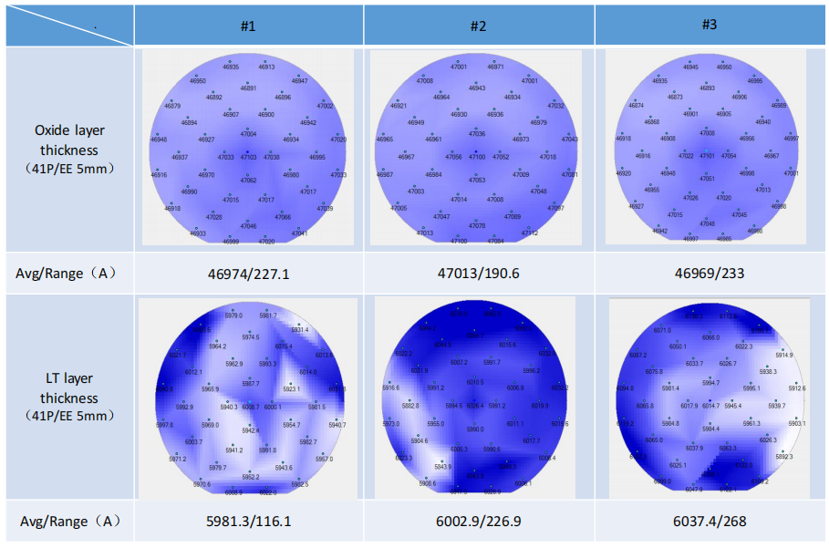
Thickness Uniformity of SiO2 and LT layer
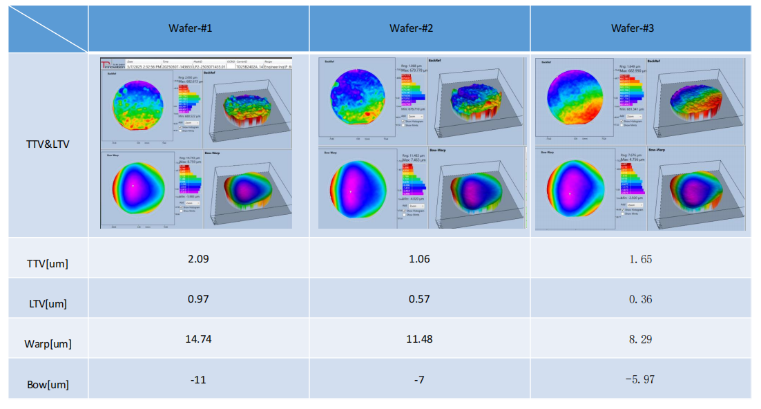
TTV BOW WRAP Data
Roughness Data

OMeda (Shanghai Omedasemi Co.,Ltd) was founded in 2021 by 3 doctors with more than 10 years of experience in nanpfabrication. It currently has 15 employees and has rich experience in nanofabrication (coating, lithography, etching, two-photon printing, bonding) and other processes. We support nanofabrication of 4/6/8-inch wafers.