I'm glad you can see this page
OMedaSemi provides cutting services. We provide two methods: wheel cutting and laser cutting. Both methods can be used for cutting chips and wafers
Wheel cutting;
*Chip and wafer cutting
*Cutting precautions; cutting path should be reserved; 300um
*Only squares can be cut
*Low cutting efficiency
Laser cutting (ordinary laser cutting and Stealth Dicing);
*Chip and wafer cutting
*Cutting path should be reserved; 100um
*Any two-dimensional plane shape can be cut,for example 8inch SOI cutted to 4inch and Chamfering
*High cutting efficiency
Processable materials;
Conventional materials; Si, Glass, Sapphire
Compound semiconductors; InP, GaAs
Crystals; LiTaO3/LiNbO3
Advanced substrates; SiC, GaN, Diamond
Thin film; Si3N4/SiO2
Size: 4 inches, 6 inches, 8 inches ,12 inches
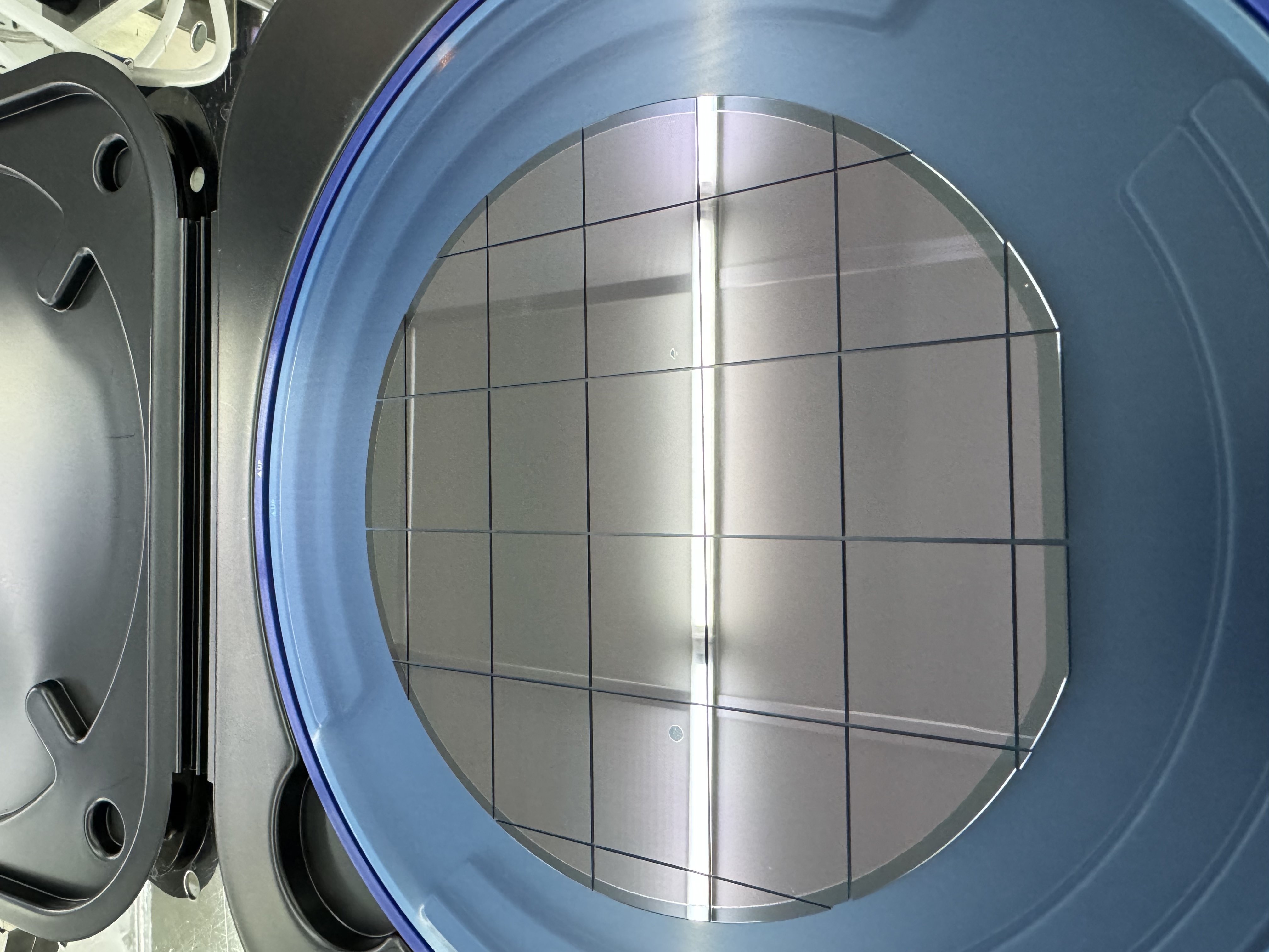
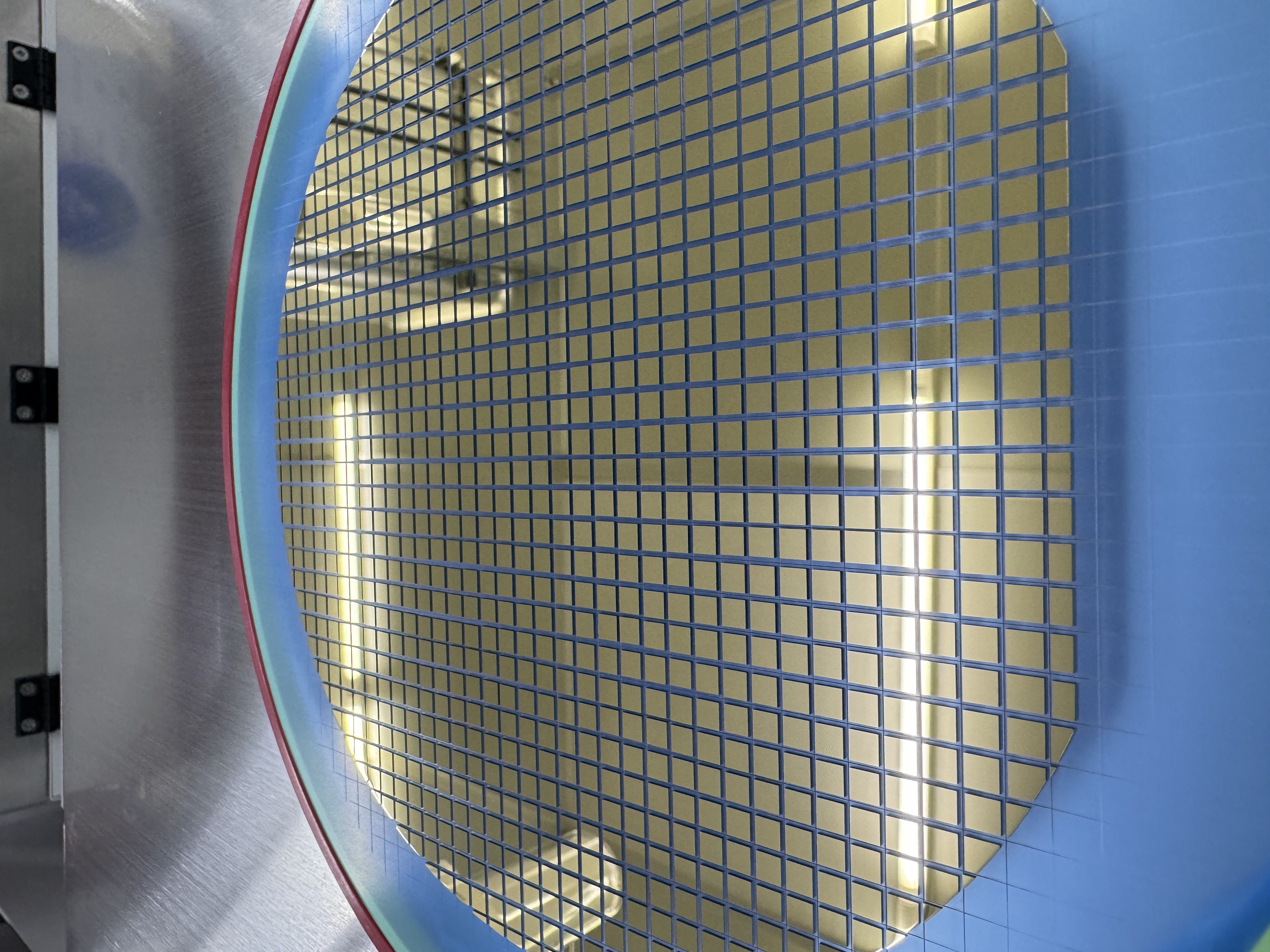
Processing case:
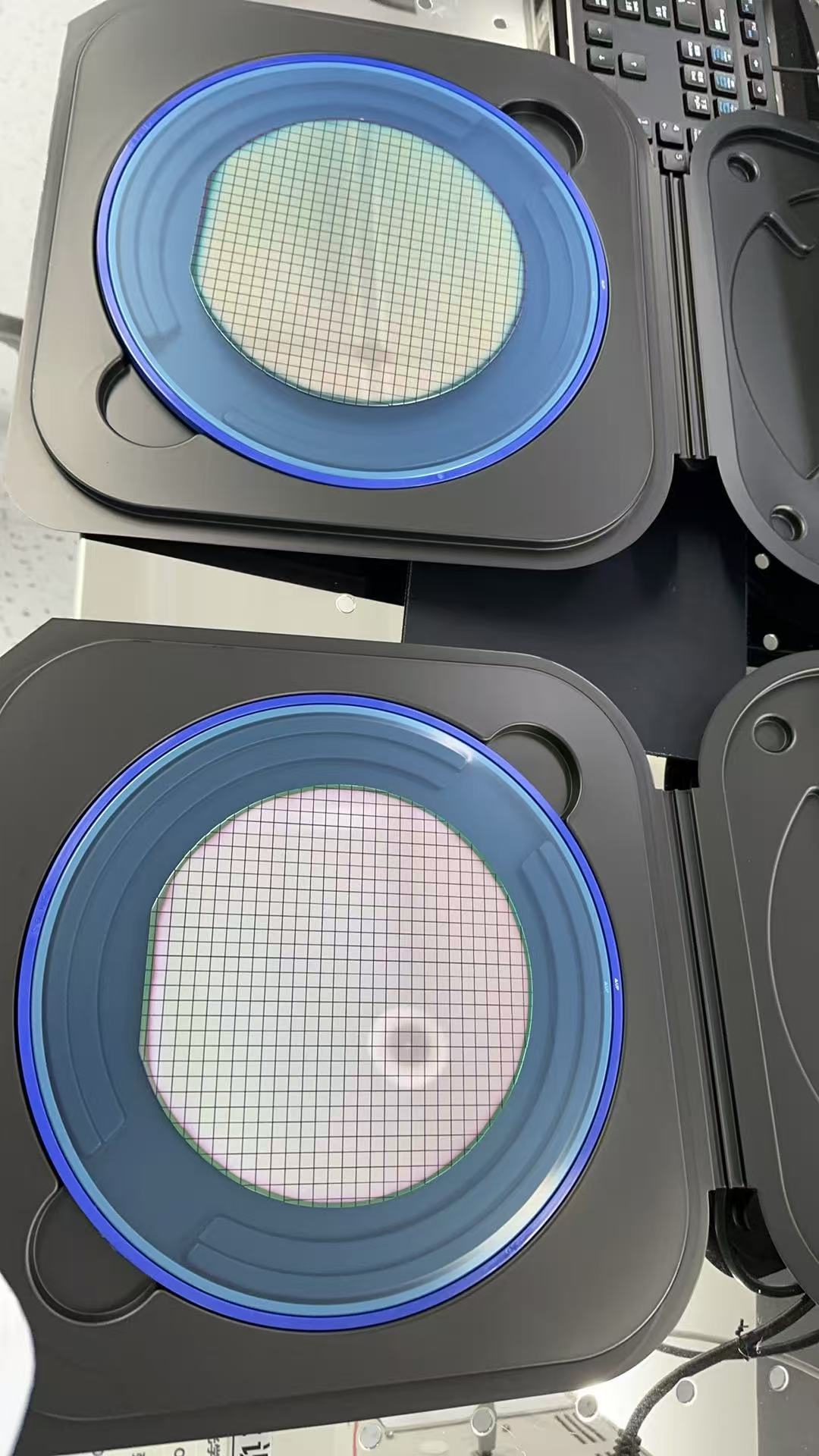
LNOI/LTOI wafer cutting
Au coated Wafer Cutting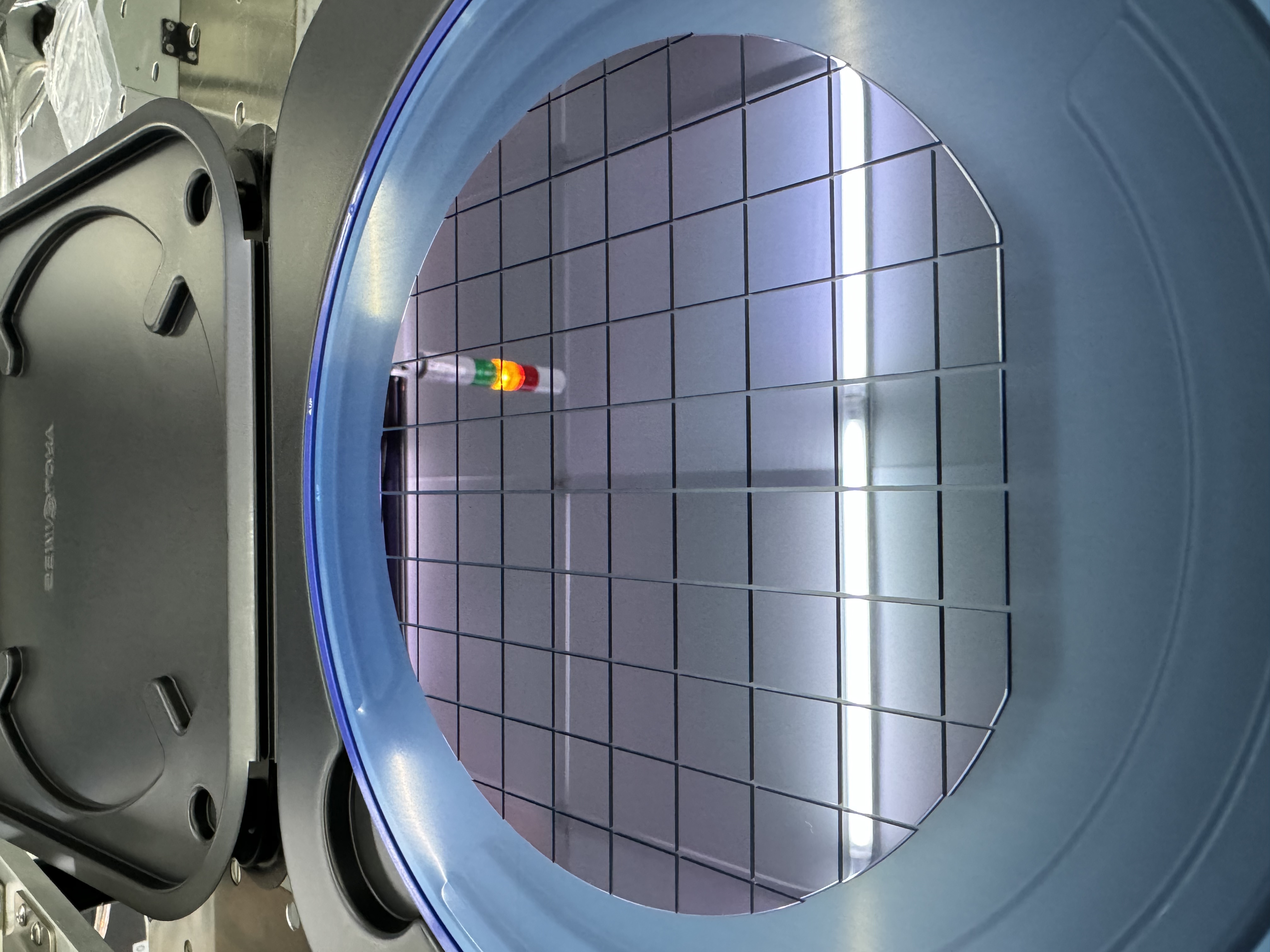
Grating wafer cutting
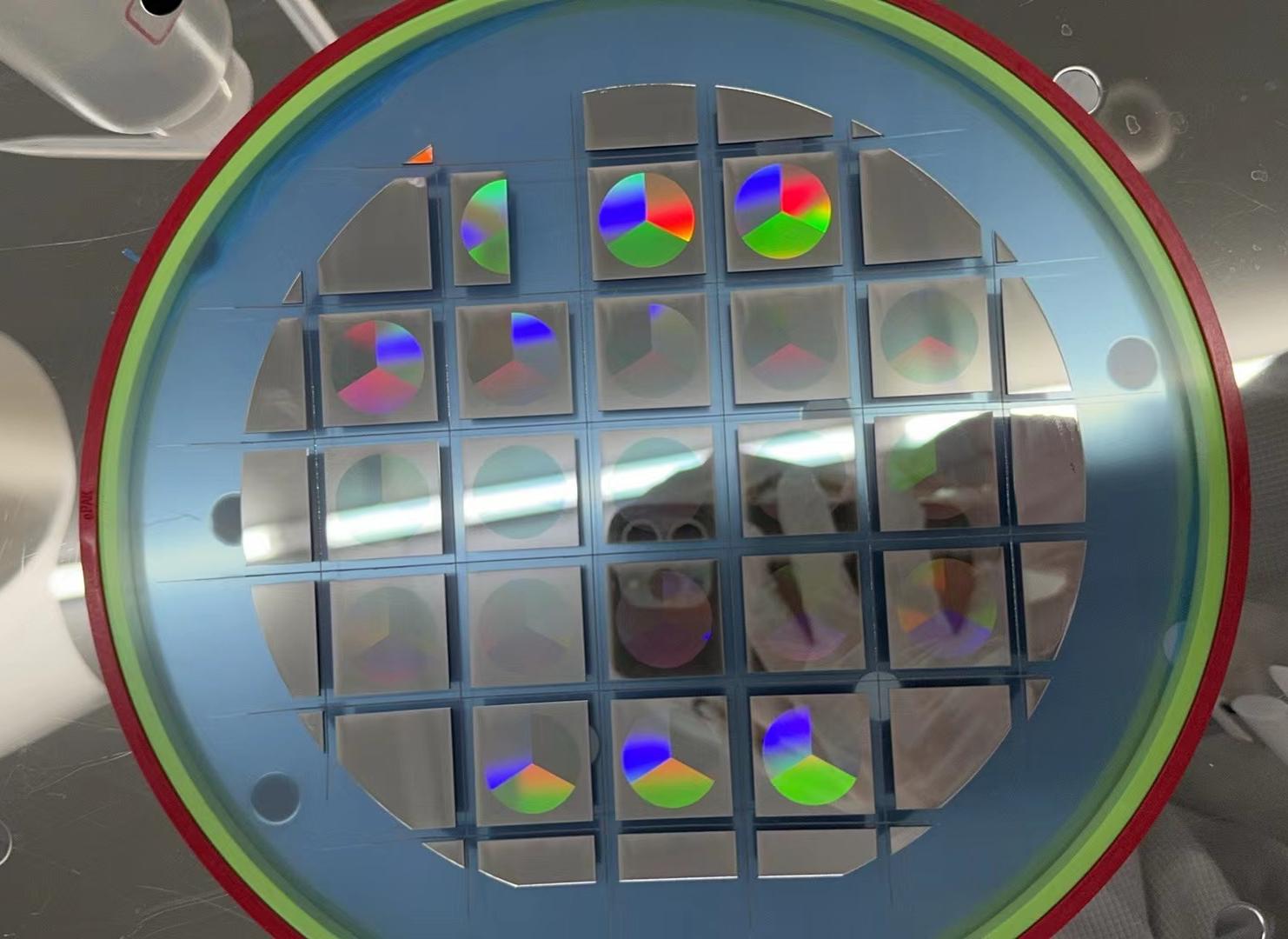
8inch SOI cutted to 4inch and Chamfering
OMeda (Shanghai Omedasemi Co.,Ltd) was founded in 2021 by 3 doctors with more than 10 years of experience in nanpfabrication. It currently has 15 employees and has rich experience in nanofabrication (coating, lithography, etching, two-photon printing, bonding) and other processes. We support nanofabrication of 4/6/8-inch wafers.