We can provide the glass wafer
About inventory
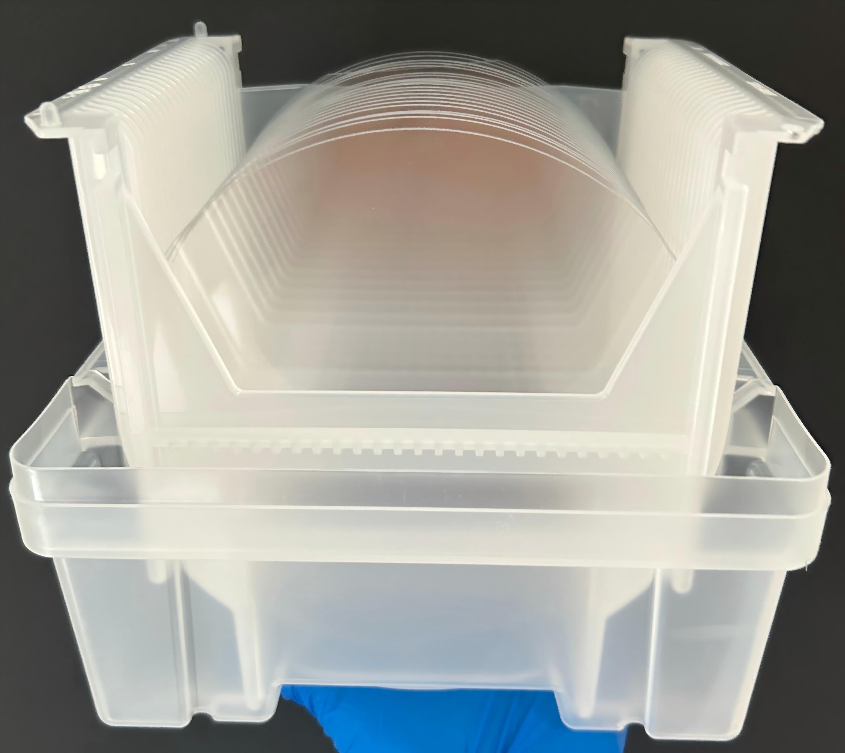
We have 6-inch 500um and 800um JGS1 wafers in stock in our warehouse. These two wafers can meet the needs of most customers
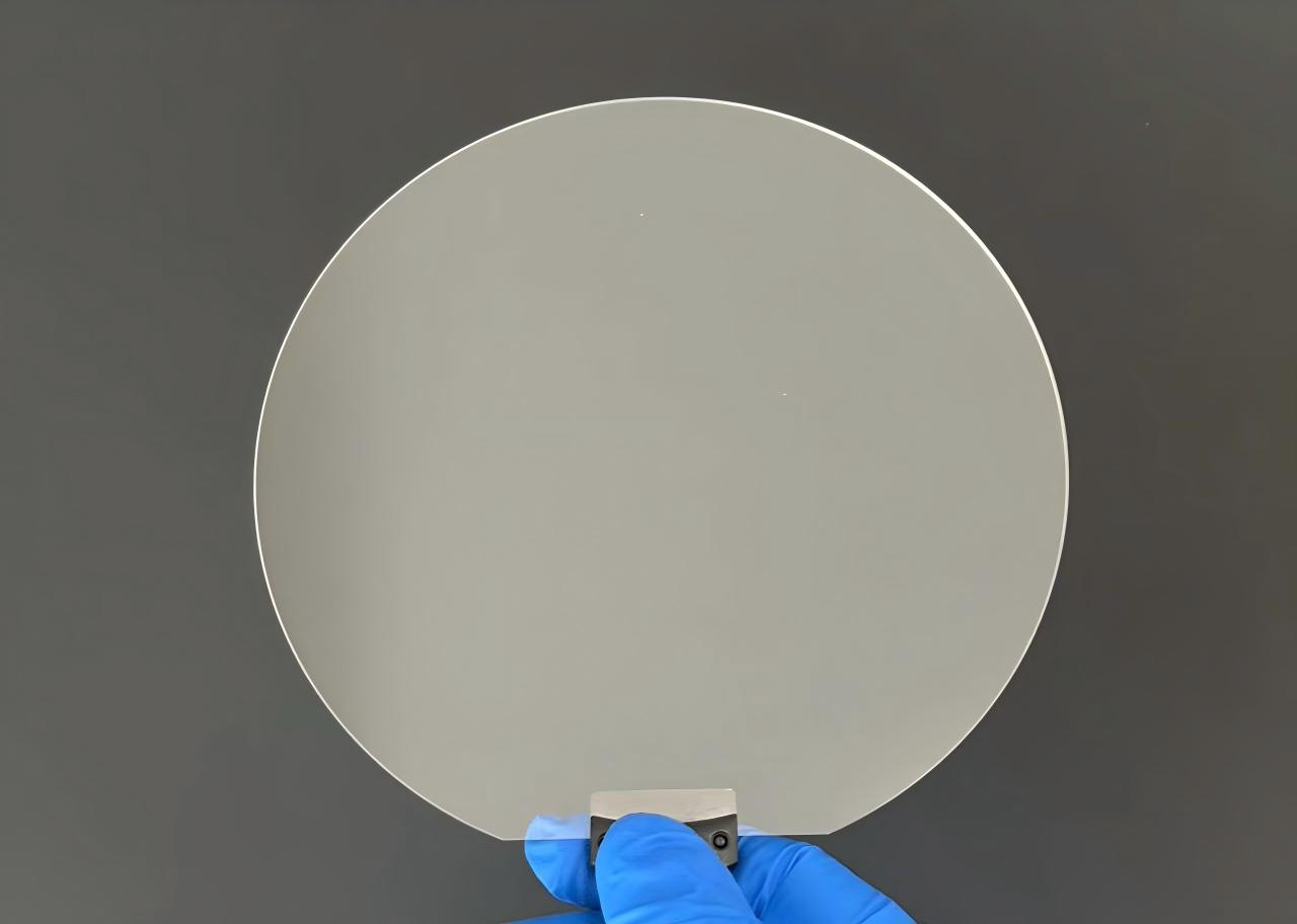
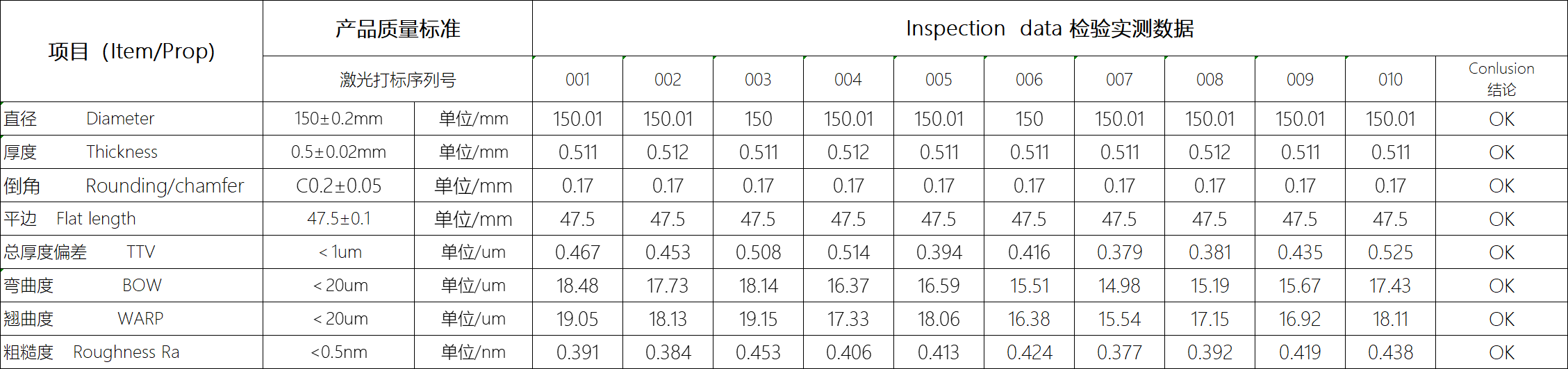
6-inch JGS1 500μm thick quartz glass wafer
 6-inch JGS1 500μm thick quartz glass wafer.pdf
6-inch JGS1 800μm thick quartz glass wafer
6-inch JGS1 800μm thick quartz glass wafer.pdf
Customized Glass Wafer Service
#Customized delivery period for conventional glass materials, such as JGS1 JGS2 JGS3, BF33, D263T, Corning Eagle, etc., is usually 1 month. The delivery period for unconventional materials = 1 month processing time cost + material purchasing time cost
#Supported size 4-inch -12-inch
BF33 6-inch x 675 glass wafer
BF33 6-inch x 675 glass wafer.pdf
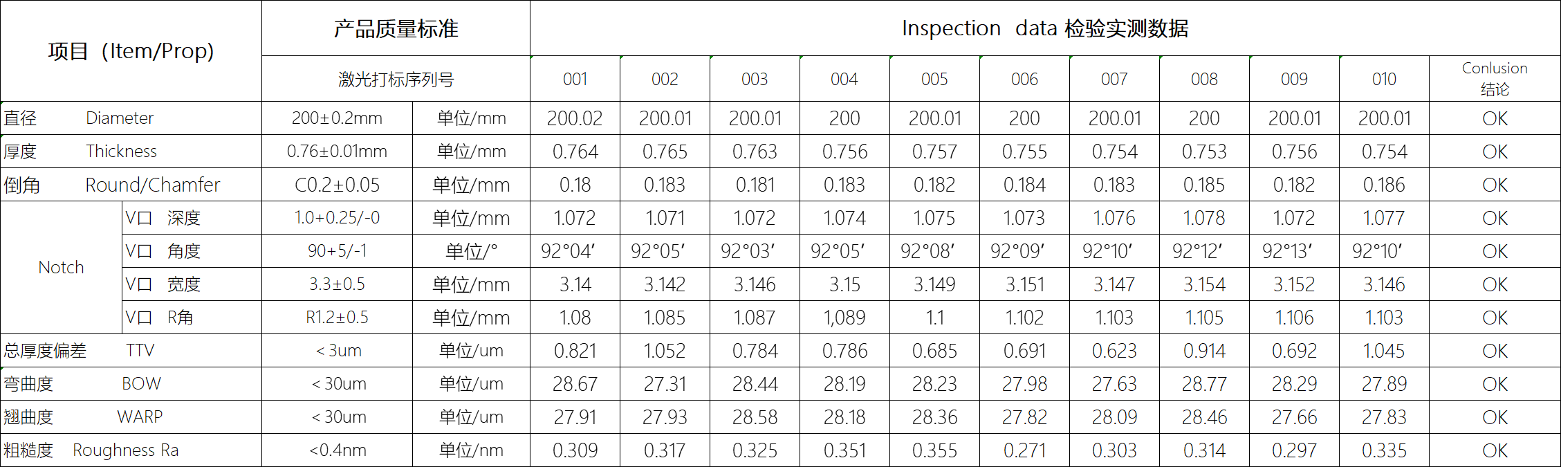
BF33 8-inch x 725 glass wafer
BF33 8-inch x 725 glass wafer.pdf
8-inch glass wafer
8寸BF33 Glass wafer(0.76mm).xlsx
About our experience:
Our company has many years of experience in the field of optics and can provide the following parameter measurement services
Refractive index, transmittance, absorption, PV, RMS, TTV, BOW, WRAP
Test data:
6inch Fused silica
8inch Bf33 Glass wafer
Conventional materials:
BF33/AF35G/JGS1/Corning 7980/Corning 7980 ARF/
High refractive index glass wafers for AR diffraction waveguides:
Hoya:
1.7 Refraction Index:
E-FD1L
1.8 Refraction Index:
NBFD15-W, FD60-W
1.9 Refraction Index:
FDS165-W
FDS24-SW
TAFD25
HOYA-TAFD25-1.9 High Refractive Index Glass Wafer.pdf
TAFD37A
FDS16-W
FDS18-W
2.0 Refraction Index:
TAFD40-W
TAFD55-W
HOYA-TAFD55-W 2.0 High Refractive Index Glass.pdf
SCHOTT:
SCHOTT RealView®
Refractive index: 1.8/1.9/2.0
Density: 3.6 (LightWeight-corresponding to lightweight applications), 4.0 (Balance), 4.5 (Standard)
CORNING:
Customized coatings
We can prepare coatings for optical applications (superstructures, optical waveguides). We can provide the corresponding refractive index data to facilitate your simulation. At the same time, our coatings have extremely high film thickness uniformity of 1%:
| Material | EBE | magnetron Sputtering | IBS | PECVD | ICPCVD | LPCVD | ALD | PLD | MOCVD | MBE |
| Au | O | O | ||||||||
| Ag | O | O | ||||||||
| Ta | O | |||||||||
| Al | O | O | ||||||||
| Cu | O | |||||||||
| Fe | O | |||||||||
| Mo | O | |||||||||
| Ti | O | O | ||||||||
| Ni | O | O | ||||||||
| W | O | |||||||||
| Ge | O | |||||||||
| Ir | O | |||||||||
| Zr | O | |||||||||
| Pt | O | O | ||||||||
| Cr | O | O | ||||||||
| NiCr | O | |||||||||
| TiW | O | |||||||||
| WC | O | |||||||||
| C | O | |||||||||
| NiSn | O | |||||||||
| AgSn | O | |||||||||
| AuSn | O | O | ||||||||
| MoS2 | O | |||||||||
| SIO2 | O | O | O | O | O | O | O | O | O | O |
| Ta2O5 | O | O | ||||||||
| TiO2 | O | O | O | |||||||
| GaO | O | |||||||||
| Ga2O3 | O | |||||||||
| Al2O3 | O | O | ||||||||
| IZO | O | |||||||||
| IGZO | O | |||||||||
| ITO | O | |||||||||
| CeO | O | |||||||||
| HfO2 | O | O | ||||||||
| NiO | O | |||||||||
| ZrO2 | O | O | O | |||||||
| Y2O3 | O | |||||||||
| WO3 | O | |||||||||
| MgO | O | O | O | |||||||
| GaN | O | |||||||||
| AlScN | O | |||||||||
| AlN | O | |||||||||
| TiN | O | |||||||||
| SiNX | O | O | ||||||||
| Si3N4 | O | O | O | |||||||
| SiC | O | |||||||||
| SiON | O | |||||||||
| Poly Si | O | |||||||||
| α Si | O | O | O | |||||||
| TEOS Sio2 | O | O | ||||||||
| SrTiO3 | O | |||||||||
| BaTiO3 | O | |||||||||
| MgF2 | O |
OMeda (Shanghai Omedasemi Co.,Ltd) was founded in 2021 by 3 doctors with more than 10 years of experience in nanpfabrication. It currently has 15 employees and has rich experience in nanofabrication (coating, lithography, etching, two-photon printing, bonding) and other processes. We support nanofabrication of 4/6/8-inch wafers.