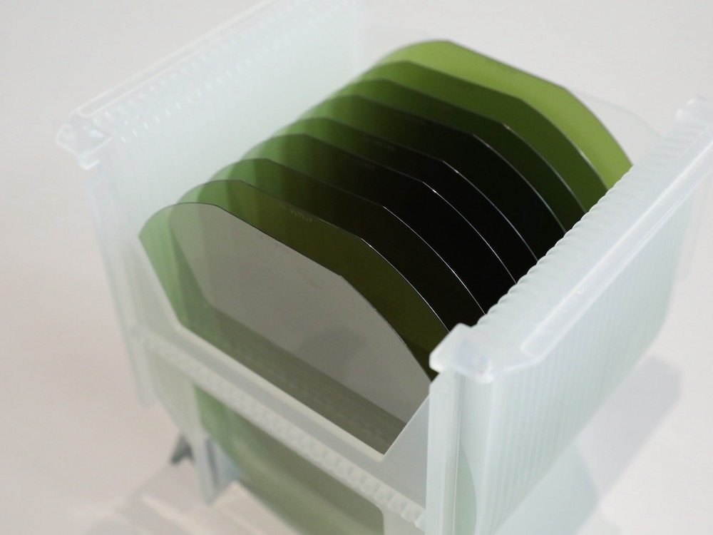
We currently provide three kinds of standard silicon carbide wafer products to the market, including N-Type Wafer ,4H HPSI Semi-Insulating Wafer (Optical Level is included ), SICOI wafer(SICOI Silicon carbide wafer on insulator)
Currently, the main specifications of products on the market are mostly the above fourtype, and other type of silicon carbide products need to be customized.
We have put the specifications of the silicon carbide products below.
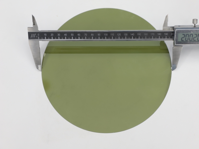
4H Semi-insulating type Wafer:
Application:
Optical Grade 4H High Purity Semi Insulating Silicon Carbide Wafer For Augument Reality Application
Delivery Time:
We have many stock ,and can ship in 4 days
SPEC
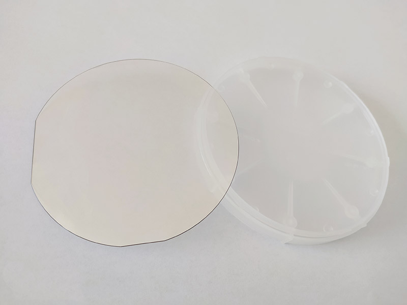
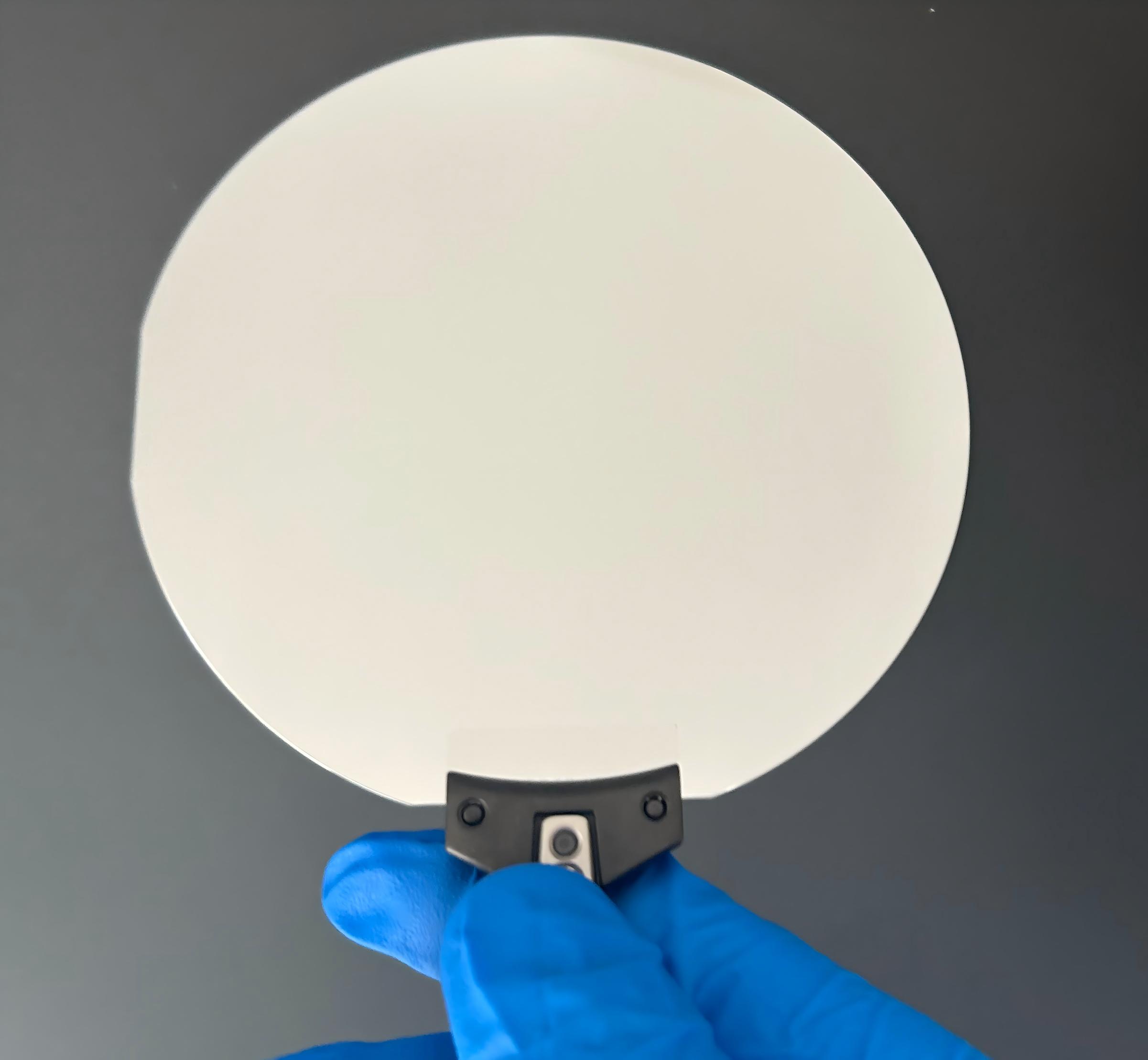
4-inch (Thickness:500um) , 6-inch (Thickness:500um) and 8 inch (Thickness:500um) semi-insulating wafers,12inch is also open for sale ,if you are interested in 12 inch 4H HPSI SIC,please contact sales to get the spec and quotation
 4inch 4H HPSI Silicon Carbide Wafer SPEC.pdf
6 inch 4H HPSI Semi Insulating Silicon Carbide Wafer Sepc.pdf
8inch 4h high purity semi insulating silicon carbide .pdf
 12 inch High Purity Semi Insulating SiC Wafer.pdf
For Optical Application
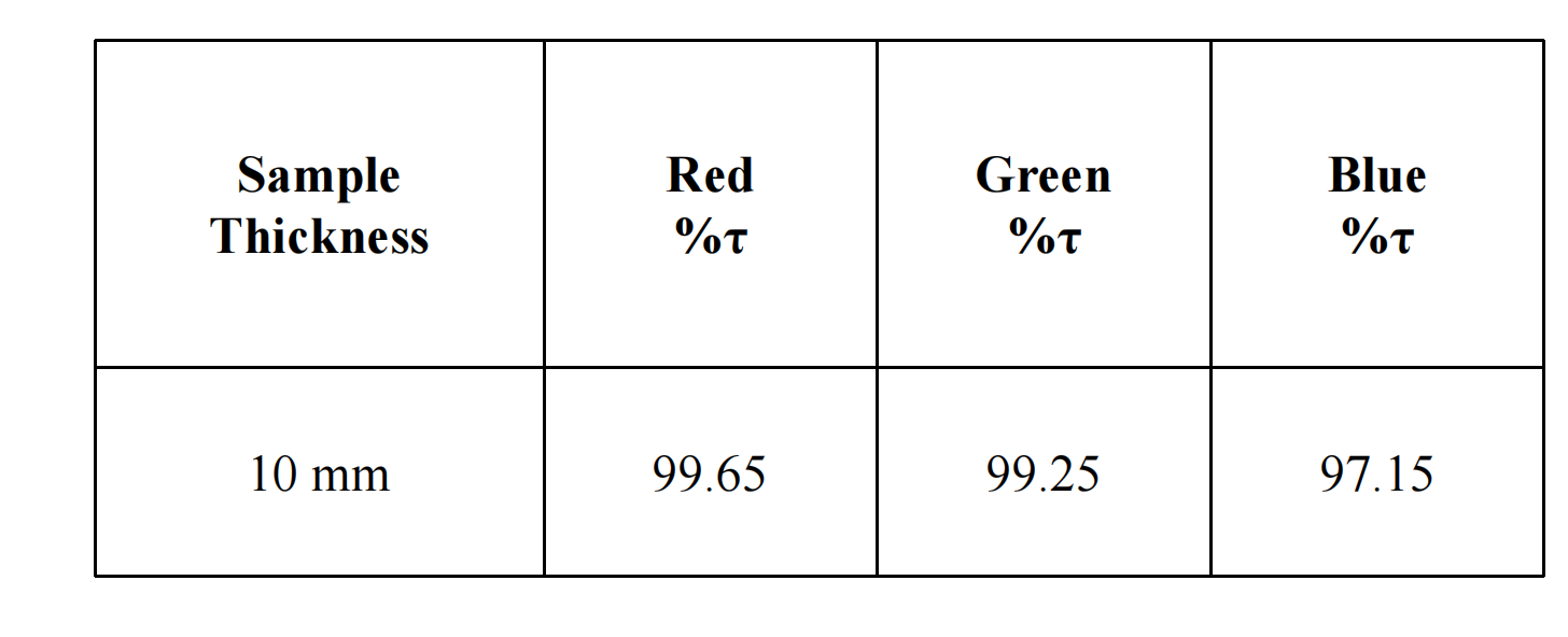
Refractive Index and Adsorption data of SIlicon Carbide:
Transmittance and absorption
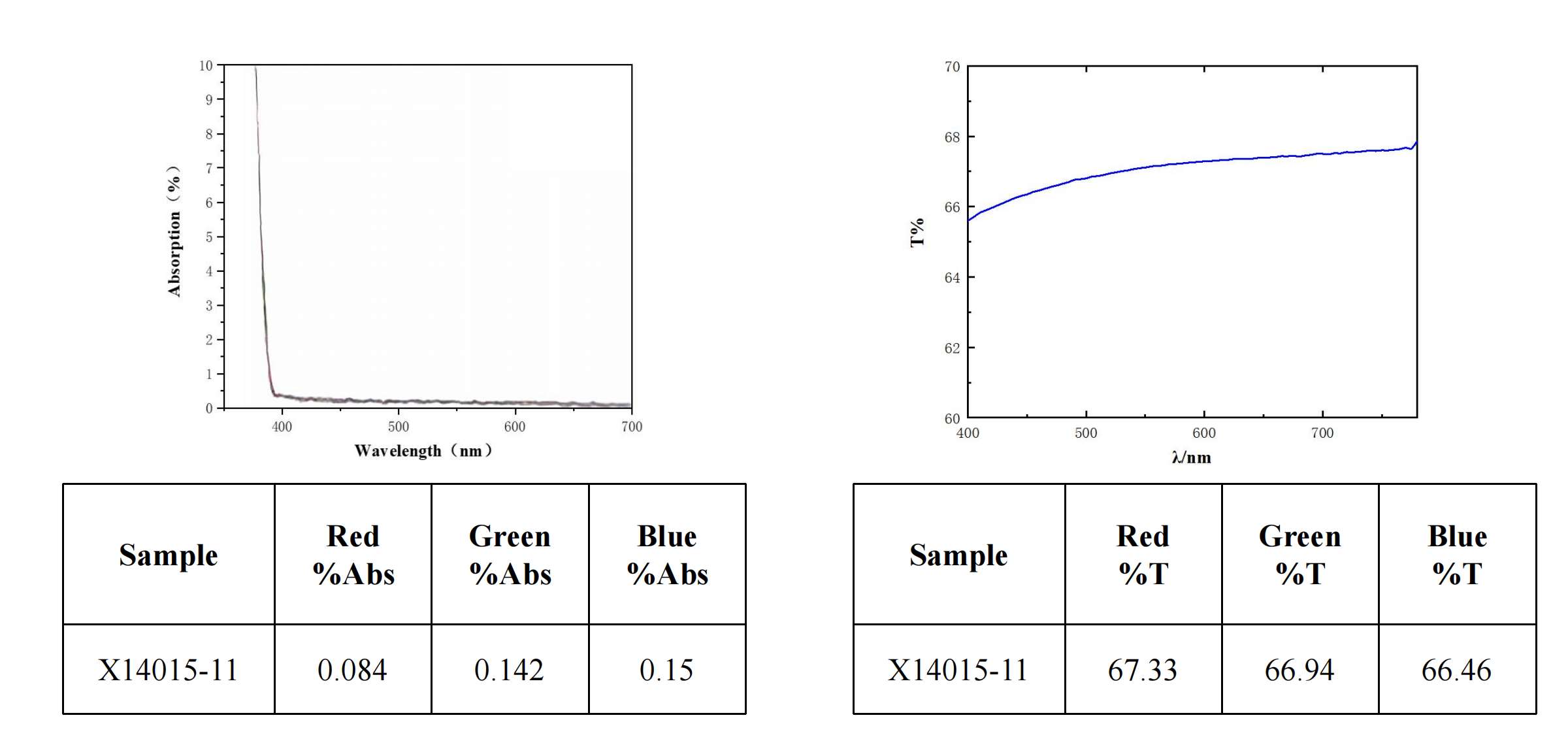
Crystal internal transmittance test(15mm Size SiC)
N type Wafer:
Delivery Time:
We have many stock ,and can ship in 4 days
SPEC
6-inch (Thickness:350um) and 8-inch (Thickness:500um) N-type conductive silicon carbide wafers
8 inch N-Type Silicon Carbide Wafer Spec.pdf
6 inch N-Type Silicon Carbide Wafer Spec.pdf
SIC EPI Wafer
Know more : please click the following link
SICOI wafer
Delivery Time
SICOI wafer is customized products ,generally we can ship to you in 4weeks
Know more : please click the following link
SICOI Wafer Silicon carbideon insulator
Cutting and Bonding Service
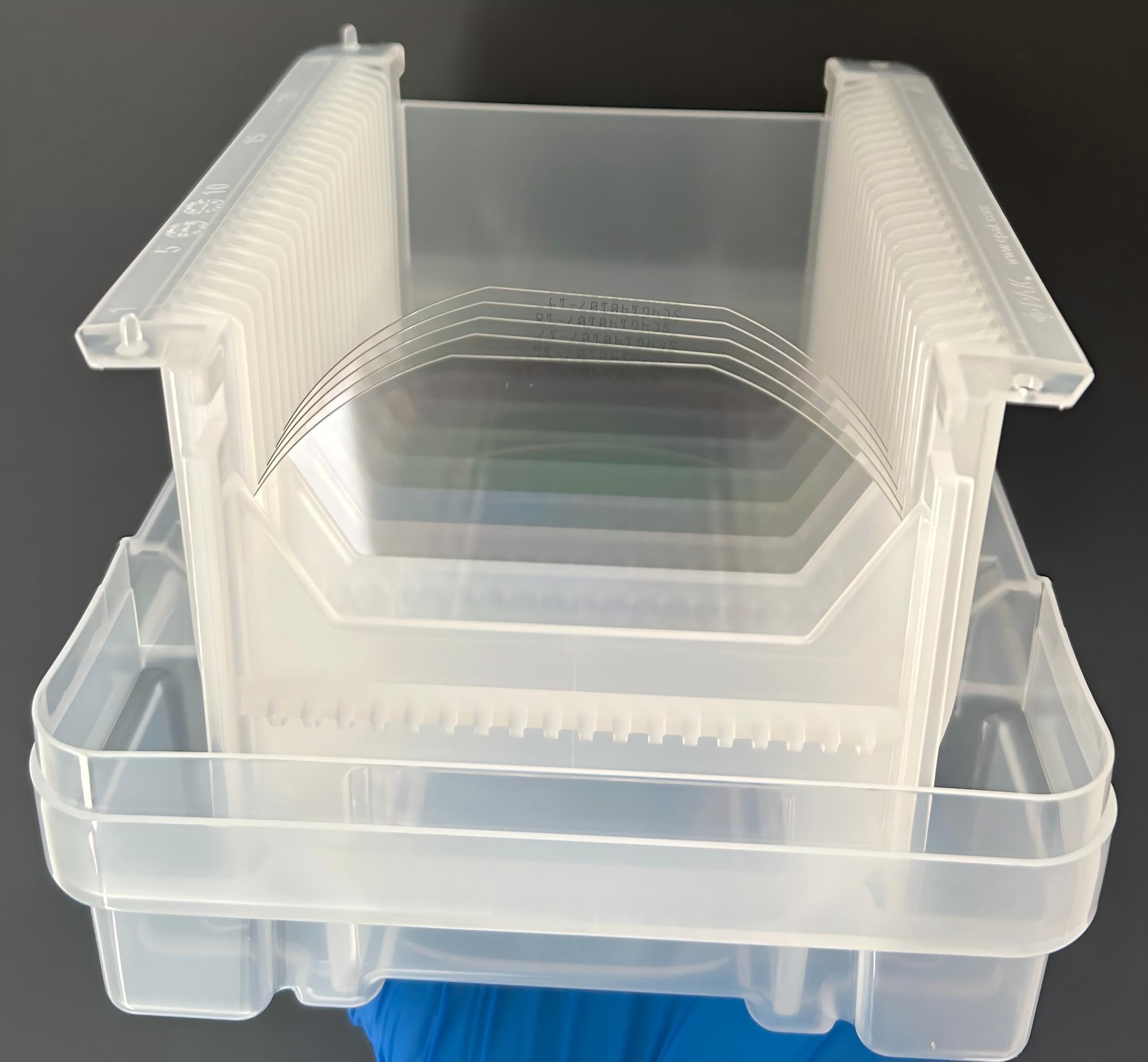
At the same time, we provide silicon carbide wafer cutting services. Cut the wafer into the size and shape you need, and you can cut round, square and other patterns.
OMeda (Shanghai Omedasemi Co.,Ltd) was founded in 2021 by 3 doctors with more than 10 years of experience in nanpfabrication. It currently has 15 employees and has rich experience in nanofabrication (coating, lithography, etching, two-photon printing, bonding) and other processes. We support nanofabrication of 4/6/8-inch wafers.