Nanoimprint Lithography
Basic Principles:
Nanoimprint Lithography (NIL) is a high-resolution, low-cost micro-nano manufacturing technology used to create nanoscale patterns and structures on the surface of materials. The following is a detailed introduction to its basic principles, classification, advantages and application areas.

Processing capabilities:
#Electron beam lithography ultra-precision master manufacturing

#UV nanoimprint lithography, up to 12 inches

Imprintable: tilted grating, straight grating, super structure, microlens array
Post-processing process: anti-reflection film, filter film, atomic layer deposition coating/evaporation coating/magnetron sputtering coating: Al2O3 aluminum oxide, HfO2 hafnium oxide, TiO2 titanium oxide, Ta2O5 tantalum pentoxide, SiO2 silicon dioxide
Process flow:
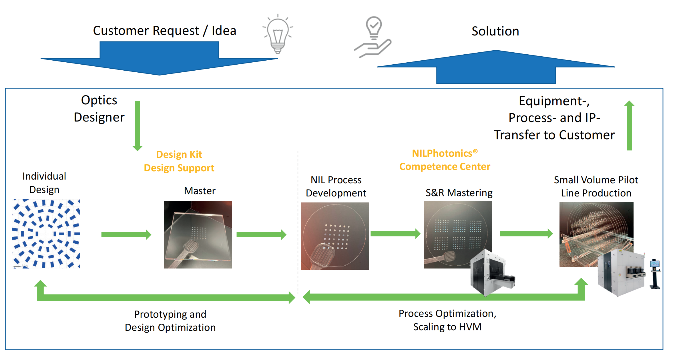
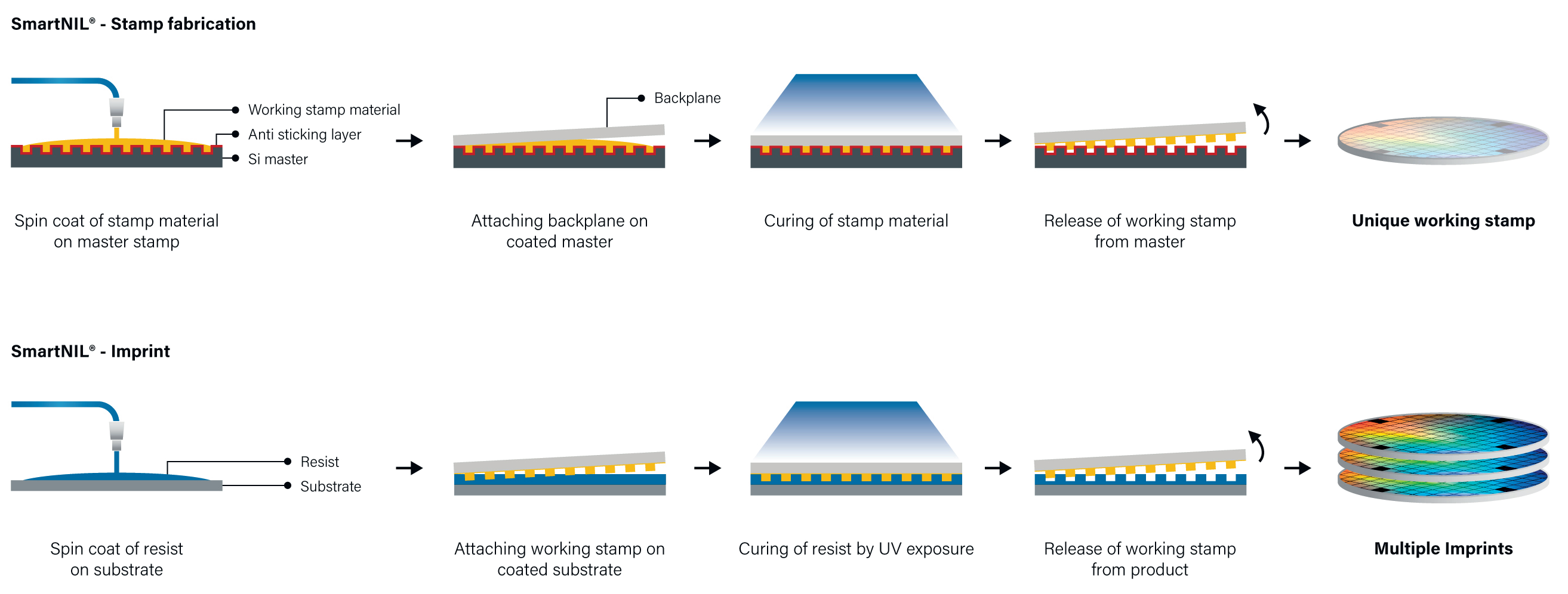
1. Mold making: Create nanoscale patterns on mold materials (such as silicon or polymers) using high-resolution techniques (such as electron beam lithography).
2. Coating resist: Coat a layer of resist (usually photoresist) on the substrate to be processed.
3. Alignment and imprinting: Align the mold with the pattern to the substrate and apply pressure to imprint the pattern on the mold onto the resist.
4. Curing: The resist is cured by ultraviolet light (UV-NIL) or heat treatment (thermal NIL), and the pattern is fixed on the substrate.
5. Demolding: The mold is removed, leaving the imprinted pattern.
6. Etching: If necessary, a subsequent etching step can be performed to transfer the pattern to a deeper layer of the substrate.
Technology classification:
Nanoimprint technology is mainly divided into the following categories:
1. Thermal Nanoimprint Lithography (T-NIL):
- Using thermoplastic polymers as resists, softening them by heating, applying pressure for imprinting, and then cooling and curing.
2. UV Nanoimprint Lithography (UV-NIL):
- Using UV-sensitive resist, applying pressure at room temperature and curing the resist by UV light.
3. Roll-to-Roll Nanoimprint Lithography (R2R-NIL):
- Using rollers instead of flat molds, suitable for large areas and continuous production.
4. Soft Nanoimprint Lithography (Soft NIL):
- Using flexible molds for imprinting, suitable for non-planar substrates.
Advantages:
1. High resolution: capable of producing patterns as small as 10 nanometers or even smaller.
2. Low cost: Compared with high-cost technologies such as electron beam lithography, nanoimprint equipment and process costs are low.
3. High efficiency: suitable for rapid replication and large-scale production of large-area patterns.
4. Simple process: The process steps are relatively simple and do not require complex optical systems.
Application areas:
1. Semiconductor manufacturing:
- Manufacturing integrated circuits and nanodevices to improve the integration and performance of devices.
2. Optical components:
- Manufacturing optical devices such as nano-gratings, microlens arrays, and reflectors for optical communications and optical imaging.
3. Biomedicine:
- Manufacturing microfluidic chips, biosensors, and cell culture substrates for biomolecule detection.
4. Storage devices:
- Used in the manufacture of high-density data storage devices such as nanodisks and nanohole arrays.
5. Flexible electronics:
- Manufacturing flexible electronic components in flexible displays, electronic paper, and wearable devices.
6. New energy:
- Making nanostructures in high-efficiency solar cells to improve light absorption and conversion efficiency.
With its advantages of high resolution, low cost, and versatility, nanoimprinting technology occupies an important position in modern micro-nano manufacturing and is widely used in many high-tech fields.
OMeda (Shanghai Omedasemi Co.,Ltd) was founded in 2021 by 3 doctors with more than 10 years of experience in nanpfabrication. It currently has 15 employees and has rich experience in nanofabrication (coating, lithography, etching, two-photon printing, bonding) and other processes. We support nanofabrication of 4/6/8-inch wafers.