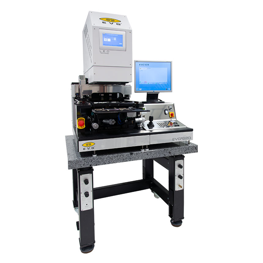
Contact lithography
When you see this page, if you have limited knowledge of this lithography method, please read this article to choose the processing method that best suits you.
Principle:
Through the optical projection system, the pattern is irradiated onto the photoresist, causing chemical changes in the photoresist, making it soluble in the solvent. The photoresist area in a specific area is removed, thereby transferring the pattern on the mask to the wafer. The ratio of the pattern on the mask to the pattern on the photoresist layer is 1:1.
Processing Capability:

• Machine:EVG 620NT
• Substrate size: small piece/2/4/6 inches
• Supports double-sided alignment and bonding alignment
• Minimum line width: 0.8 μm
• Light intensity uniformity: ≤3%
• Front alignment accuracy: ≤0.5 μm
• Back alignment accuracy: ≤1 μm
OMeda (Shanghai Omedasemi Co.,Ltd) was founded in 2021 by 3 doctors with more than 10 years of experience in nanpfabrication. It currently has 15 employees and has rich experience in nanofabrication (coating, lithography, etching, two-photon printing, bonding) and other processes. We support nanofabrication of 4/6/8-inch wafers.

