I am glad that you can see this page.
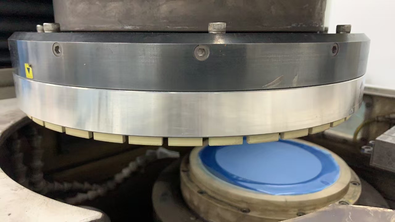
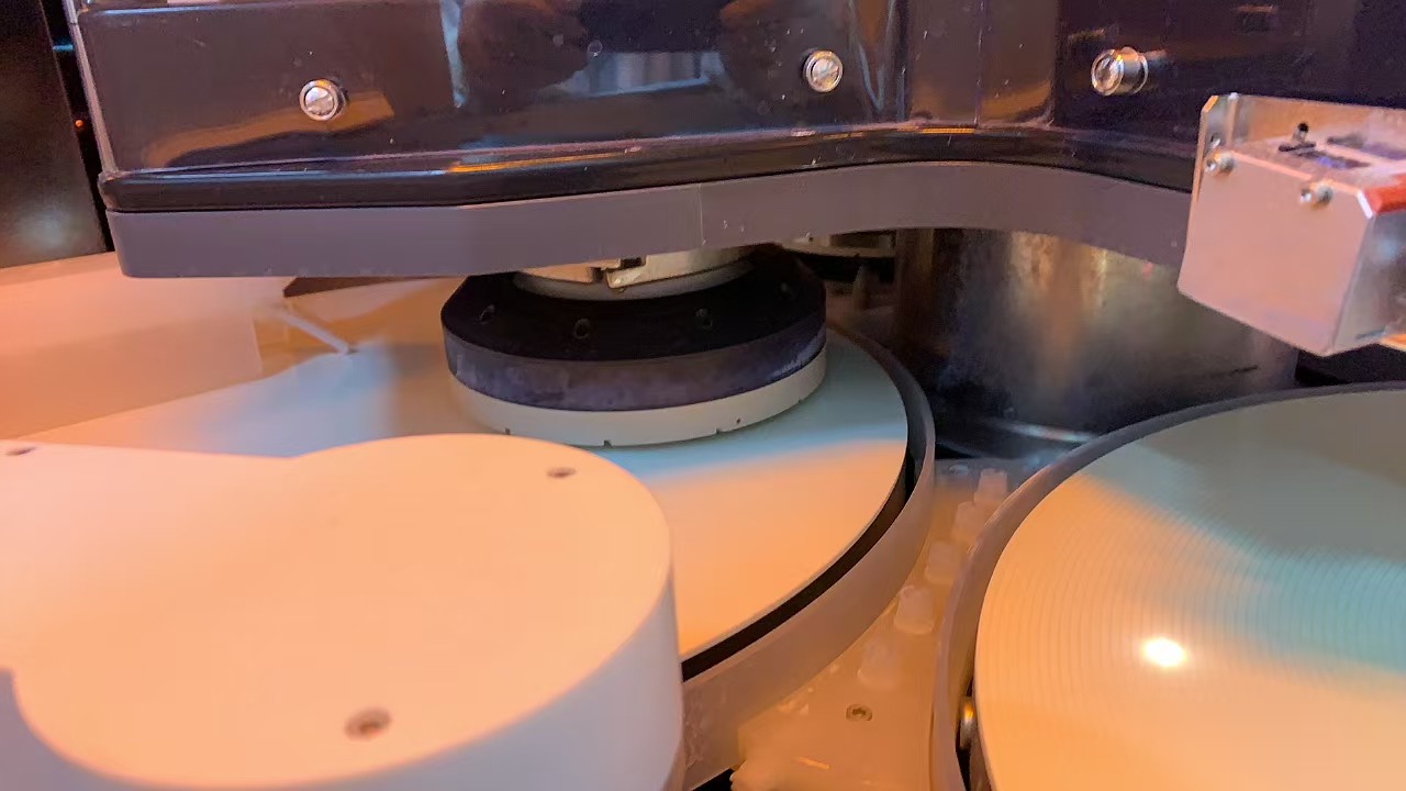
OMedaSemi provides mechanical thinning and chemical mechanical polishing services. In semiconductor processing, mechanical thinning process is widely used. For example, after the cladding growth in photonic integrated circuits, the top cladding needs to be chemically mechanically polished to reduce the roughness of the cladding. In the preparation of thin-film lithium niobate and SOI wafers, the material needs to be thinned and polished before and after the bonding process. In the preparation of wafers, the wafers after wire cutting need to be chemically mechanically polished before the post-processing.
However, the industry lacks professional and reliable suppliers of mechanical thinning and chemical mechanical polishing processing
Grinding thinning:

Materials:
Conventional materials; Si, Glass, Sapphire
Compound semiconductors; InP, GaAs
Crystals; LiTaO3/LiNbO3
Advanced substrates; SiC, GaN, Diamond
Thin films; Si3N4/SiO2
Size: 4 inches, 6 inches, 8 inches
CMP polishing:

Material requirements:
Conventional materials; Si, Glass, Sapphire
Compound semiconductors; InP, GaAs
Crystals; LiTaO3/LiNbO3
Advanced substrates; SiC, GaN, Diamond
Thin films; Si3N4/SiO2
Size: 4 inches, 6 inches, 8 inches
OMeda (Shanghai Omedasemi Co.,Ltd) was founded in 2021 by 3 doctors with more than 10 years of experience in nanpfabrication. It currently has 15 employees and has rich experience in nanofabrication (coating, lithography, etching, two-photon printing, bonding) and other processes. We support nanofabrication of 4/6/8-inch wafers.

