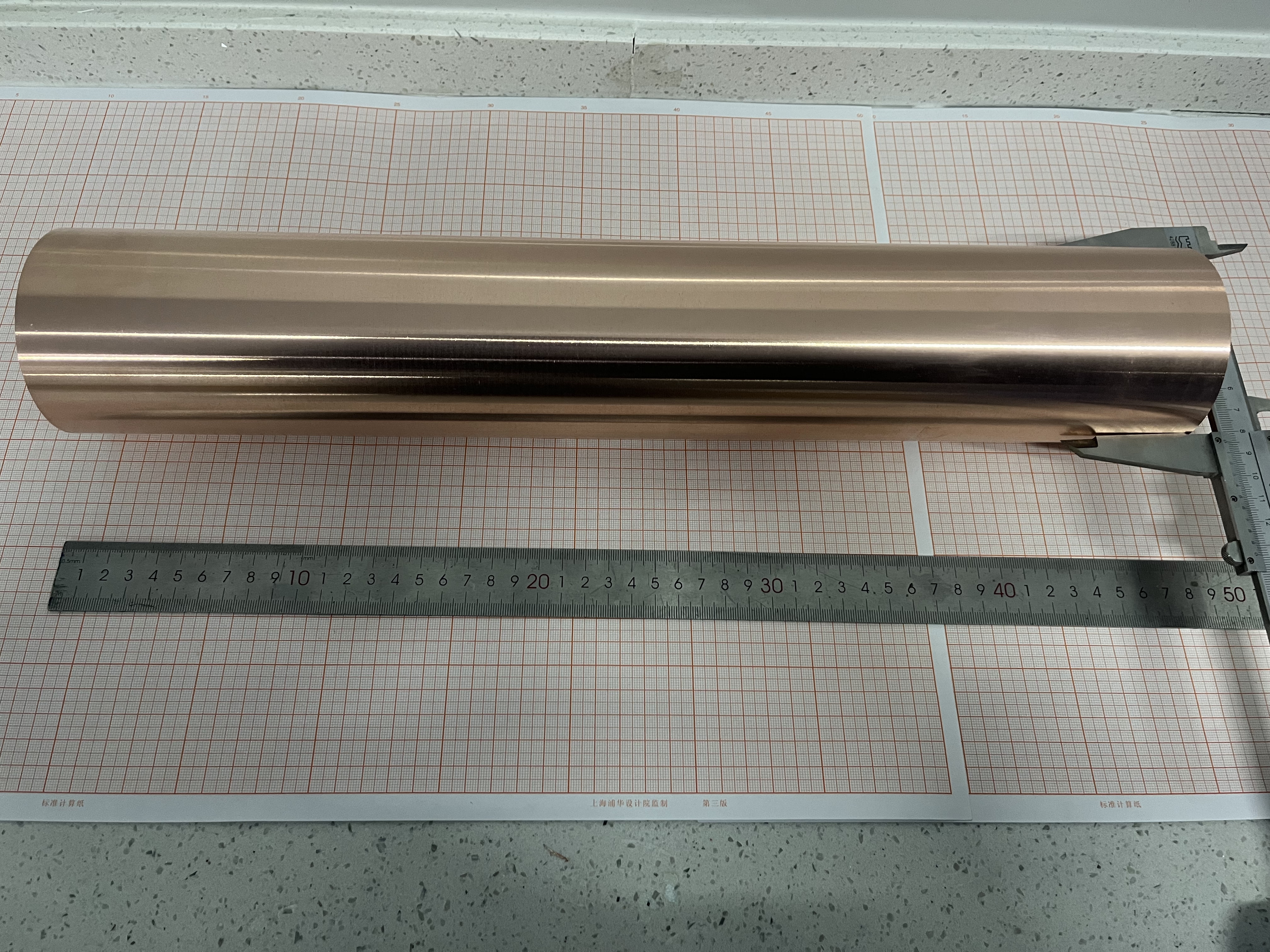
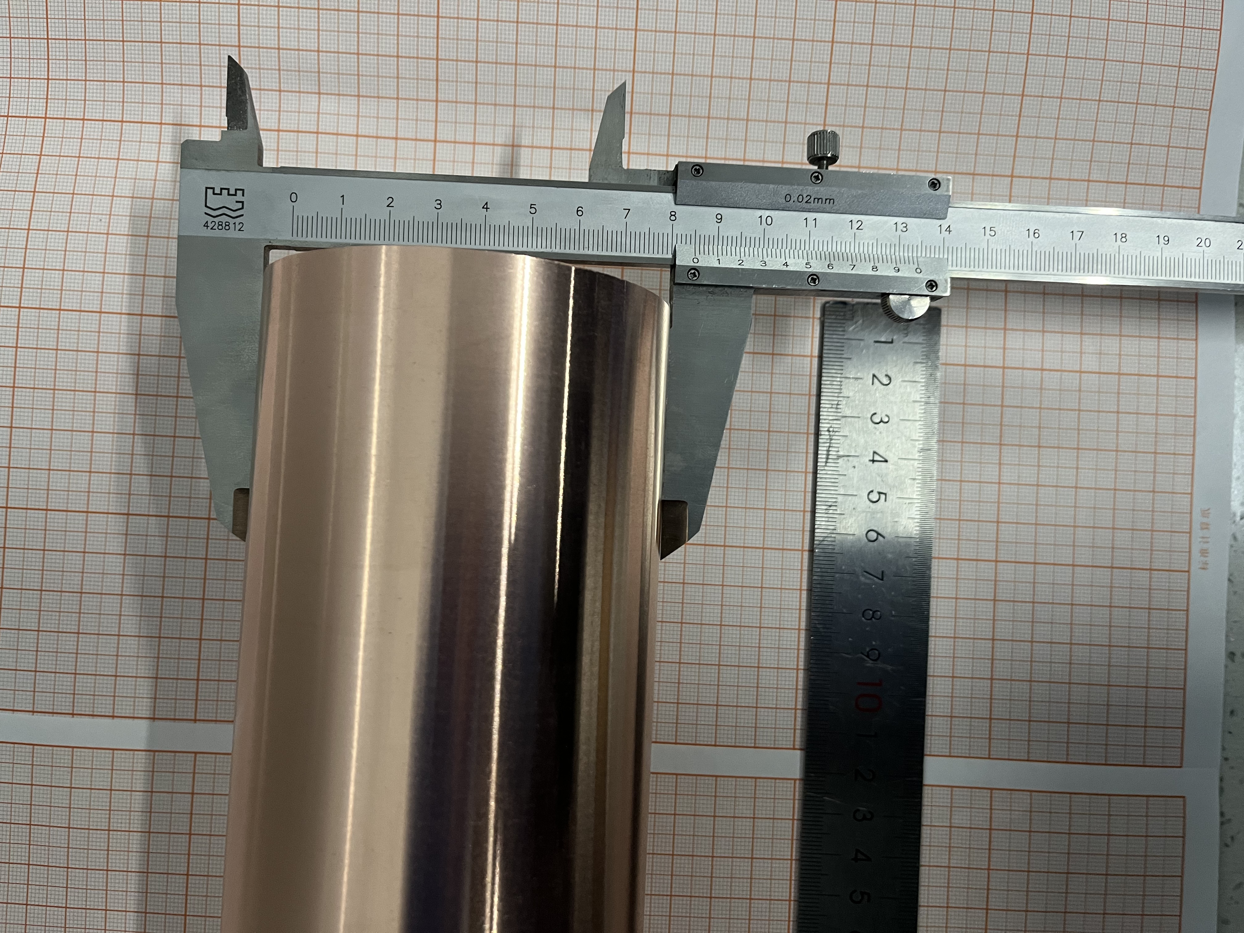
OMedaSemi can provide single crystal copper materials, real single crystal copper,
Purity is 7N,max size is 4inch
Single Crystal Copper:
Copper (Cu) is the most widely used conductive and thermal conductive material in the world. Due to its low price and excellent conductive properties, it is widely used in production and life;
Single crystal copper is a high-purity copper composed of only one grain, and there is no "grain boundary" between grains;
Excellent electrical and signal transmission performance, good plastic processing performance; excellent corrosion resistance; significant fatigue resistance; mainly used in defense high technology, civil electronics, communications and networks.
Advantages of single crystal copper:
#No grain boundary--with extremely high signal transmission performance
#Good plastic processing--higher elongation than ordinary polycrystalline copper
#High toughness--single crystal TTF116 turns, better than 50 turns of ordinary copper
#Low resistivity--reaching 116%IACS, better than silver
#1. The purity of single crystal copper reaches 99.9999%
During the manufacturing process, high vacuum is used to melt the raw materials. The vacuum degree during the melting process is as high as 10-4Pa, which can effectively remove gas impurities and low melting point impurities in the raw materials;
#2. The resistance is 8% to 13% lower than that of ordinary copper
Single crystal copper eliminates lateral grain boundaries, improves purity, and avoids casting defects, thereby reducing the damage to the directional movement of electrons caused by the collision of free electrons with grain boundaries, impurities, defects, etc. during movement, and reducing the resistivity of single crystal copper.
3. Excellent low temperature characteristics
It has the smallest grain boundary area and few lattice defects. The residual resistivity (RRR=ρ293K/ρ42K) of high-purity single-crystal copper is about 20 times higher than that of ordinary copper.
4. Dense organization Reaching the theoretical density of copper of 8.932g/cm3, the crystal also grows in a completely long-range orderly manner along a specific direction, with a stable crystal structure and dense organization, and avoiding the generation of casting defects. The prepared ultra-fine wire has a smooth surface quality.
5. High ductility Ordinary copper material breaks after 16 twists, while single-crystal copper material can be twisted 116 times. The cold rolling deformation rate of high-purity single-crystal copper reaches more than 6000%. A single-crystal copper rod with a diameter of Ф8mm can be rolled into a 0.006mm copper foil without any annealing.
6. Low cost Single crystal copper wire costs only 1/3-1/10 of gold wire, which can save 90% of the cost of bonding packaging materials; the specific gravity is 1/2 of gold wire, and 1 ton of single crystal copper wire can replace 2 tons of gold wire
Application:
#Graphene epitaxial substrate
#Target material--magnetron sputtering single crystal copper target
#Wire
--As a conductor--reduce heat generation, such as electric vehicle charging cables, etc.
--Audio signal transmission--audio signal fidelity
OMeda (Shanghai Omedasemi Co.,Ltd) was founded in 2021 by 3 doctors with more than 10 years of experience in nanpfabrication. It currently has 15 employees and has rich experience in nanofabrication (coating, lithography, etching, two-photon printing, bonding) and other processes. We support nanofabrication of 4/6/8-inch wafers.