Monocrystalline Polycrystalline Diamond Wafer
We can supply MPCVD monocrystalline and polycrystalline diamond materials.
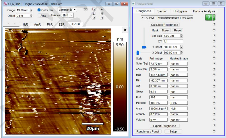
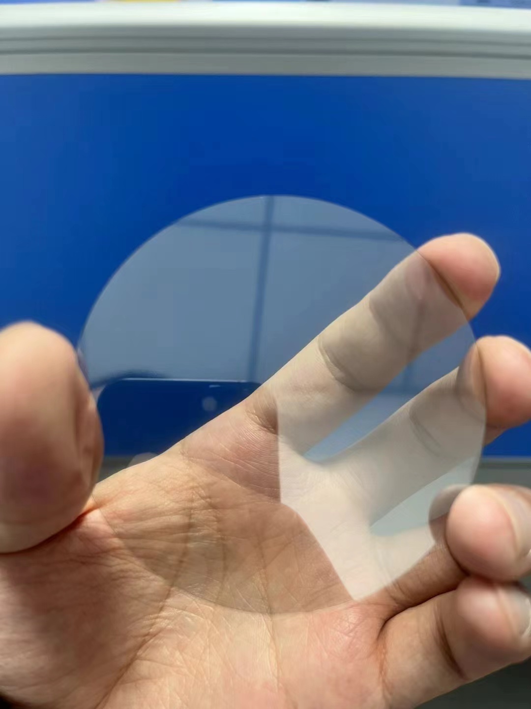
Ultra Smooth Polishing Process :
OMedaSemi Develop special process for diamond wafer ,
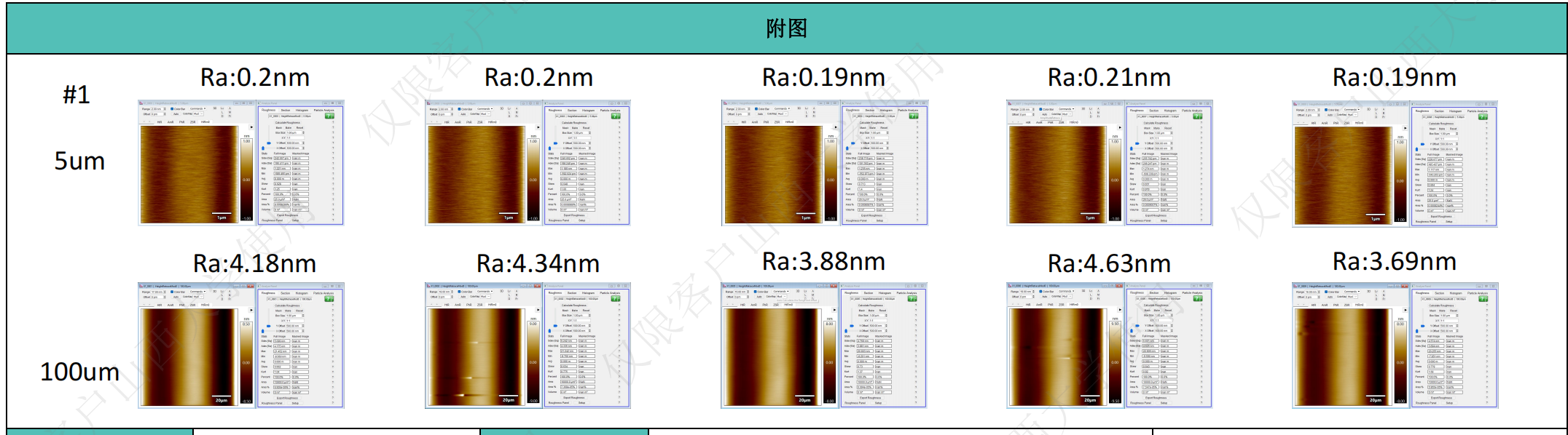
For monocrystalline wafer ,we provide 3 kind of roughness level Diamond :
Level 1:2nm
Level 2:1nm
Level 3:0.5nm
Level 4:0.3nm--High Price
Level 5:0.1-0.2nm--High Price
poly CRYSTALP olishing
For monocrystalline wafer ,we provide 3 kind of roughness level Diamond :
Level 1:10nm
Level 2:5nm
Level 3:1nm--High Price
Level 4:0.5nm--High Price
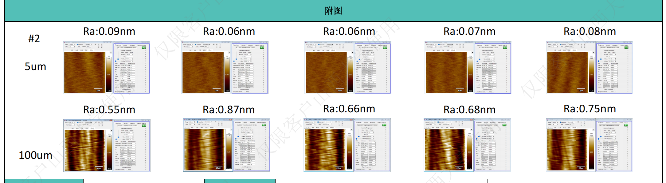
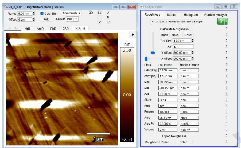
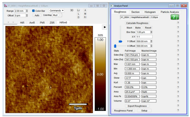
(Before:Ra1.17nm After:Ra0.42nm)(5um*5um)
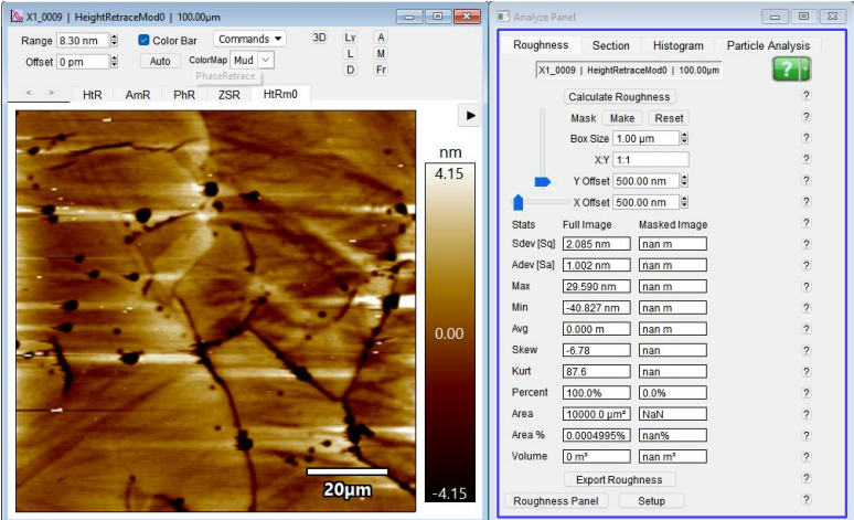
(Before:Ra2.68nm After:Ra1nm)(100um*100um)
Purchase Guide (Mandatory Reading)
We are glad that you have reached this page. We recommend that you read through the following information carefully before contacting our sales representatives.
If you are purchasing diamond products for the first time, please confirm the information below in detail and then provide it to our sales team.
Monocrystalline Diamond or Polycrystalline Diamond?
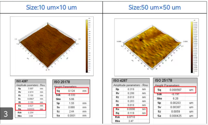
Differences Between Monocrystalline and Polycrystalline Diamonda. For small-sized products (≤10×10 mm), the unit price of monocrystalline diamond is similar to that of polycrystalline diamond. However, polycrystalline diamond can be grown up to 6 inches in size, while the maximum size of monocrystalline diamond available domestically is only 2 inches currently. Therefore, if you are purchasing large-sized diamond and have a limited budget, polycrystalline diamond is recommended as the priority option.b. Monocrystalline diamond has higher thermal conductivity.c. Monocrystalline diamond is easier to polish than polycrystalline diamond. Monocrystalline diamond can be polished to a roughness of 0.5 nm–2 nm, whereas polycrystalline diamond requires ion beam refinement to achieve the same level of roughness. Generally, the roughness of polished and lapped polycrystalline diamond is 5 nm–10 nm.
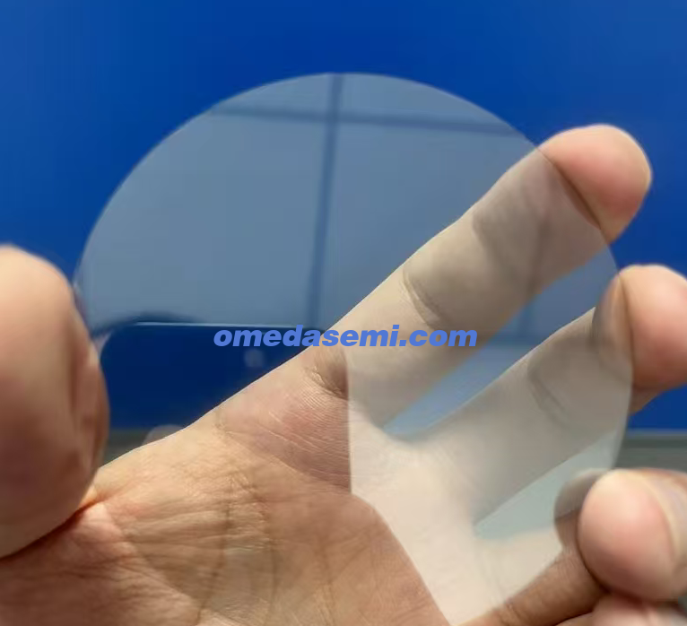
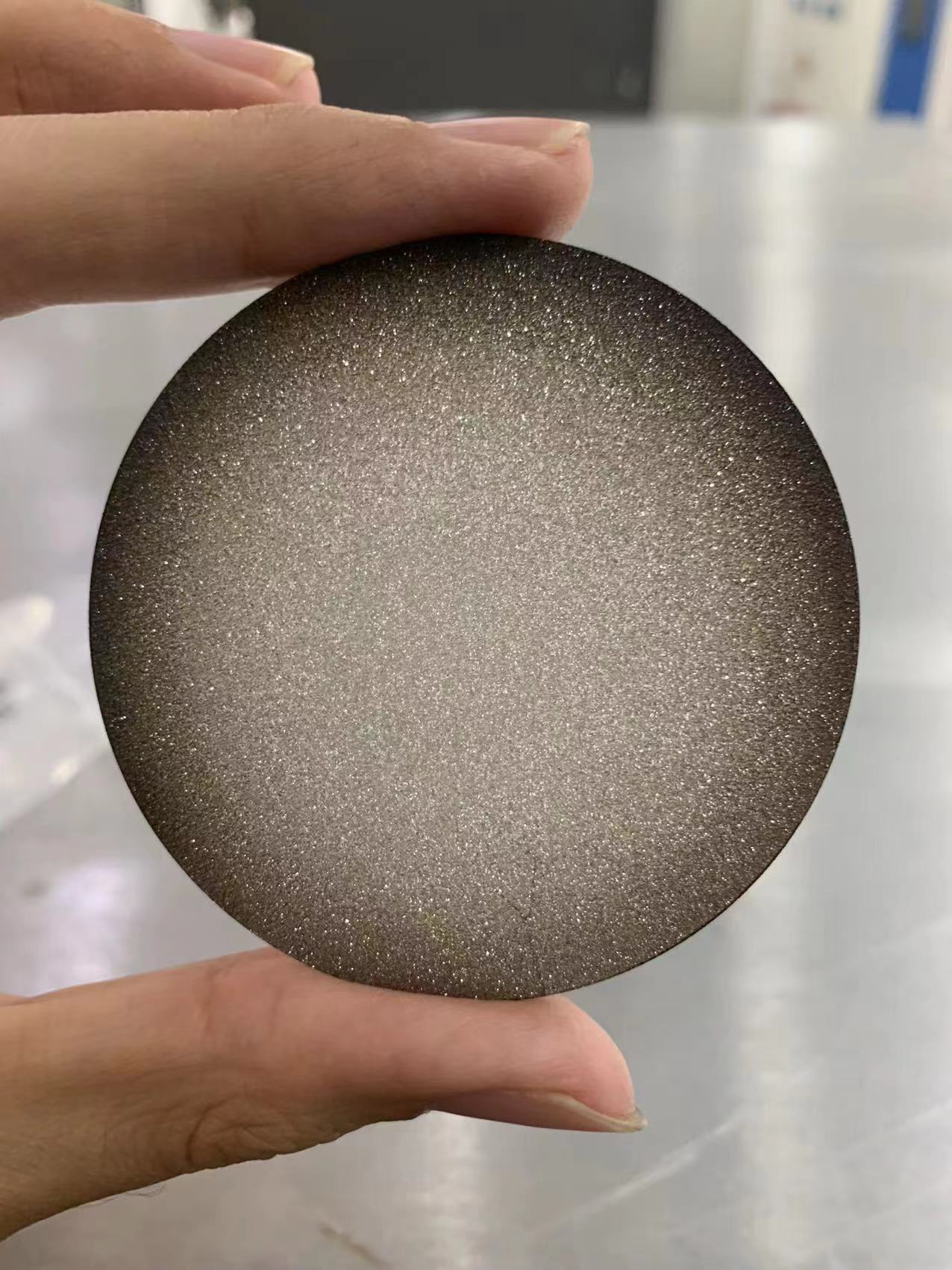
2. Optical Grade or Thermal Grade
Both single-crystal and polycrystalline diamonds are divided into optical grade and thermal grade diamonds. The difference is that optical grade diamonds are transparent and have fewer impurities and black spots in the crystal. The differences are shown in the image below.
Thermal grade:
Optical Grade:
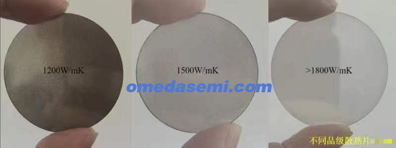
3. Which grade of thermal grade diamond to choose
Whether it's polycrystalline or single-crystal diamond, thermal conductivity is generally divided into four levels: 1200 W/m·K, 1500 W/m·K, 1800 W/m·K, and 2000 W/m·K. Higher thermal conductivity means a higher price.
4. Do you have diamonds with a {111} crystal orientation?
The largest size of {111} crystal orientation diamond we can currently provide is 5mm x 5mm, single-crystal diamond with {111} orientation.
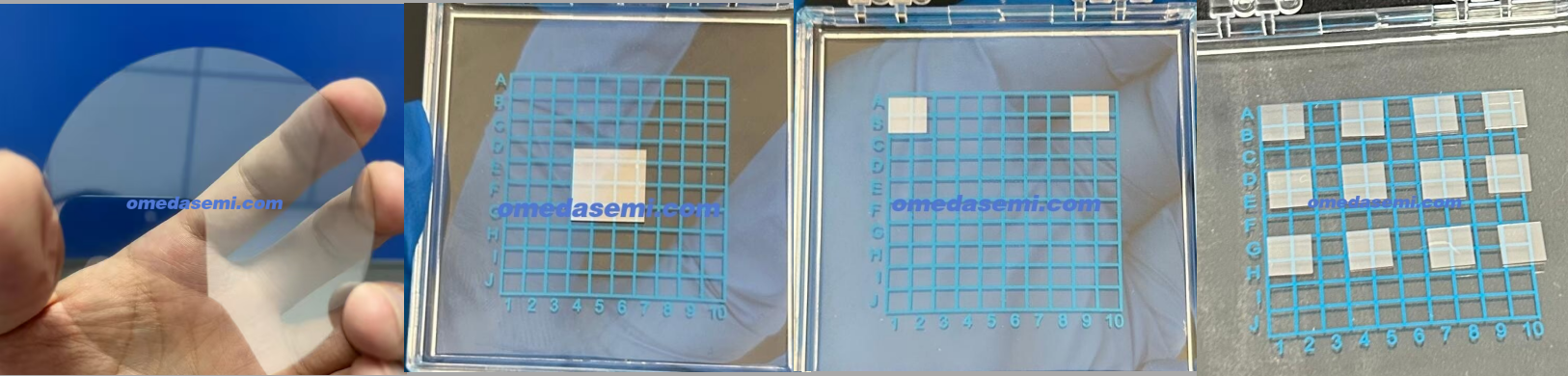
5.Which sizes and thicknesses of diamonds should I choose?
For single-crystal diamonds, we can generally provide up to 1 inch in size, while for polycrystalline diamonds, we can provide up to 4 inches. The typical thickness is 0.3mm or 0.5mm. For thicker diamonds, regrowth is required. The thinnest diamond we can achieve is 0.1mm.
If this is your first time using them, we recommend purchasing 10x10mm - 0.5mm single-crystal or polycrystalline diamonds.
6.Should I choose single-sided polishing, double-sided polishing, or just grinding?
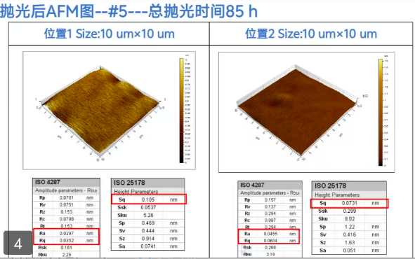
The processing flow for diamonds is grinding - polishing. After grinding, the roughness of polycrystalline diamonds is 200-500nm, and after polishing, the roughness reaches 5-10nm. After cutting single-crystal diamonds (with laser cutting marks), the roughness is 200-500nm. After grinding (matte surface, without laser cutting marks), the roughness is 100-500nm. After polishing, the roughness can reach 0.5-2nm.
Polycrystalline diamonds can be ion-beam polished to below 0.5nm, and single-crystal diamonds can be ion-beam polished to below 0.3nm.
"Therefore, when you decide to purchase diamonds, please confirm the following:
Optical grade or thermal grade (what is the required thermal conductivity?)
Size, size tolerance (default tolerance is ±0.1mm unless otherwise specified), thickness, thickness tolerance (default tolerance is ±0.30μm unless otherwise specified)
TTV (Total Thickness Variation), Warp (leave blank if no specific requirement)
Single-sided polishing, double-sided polishing, or just grinding, roughness requirements
Quantity needed
If you're still uncertain, we recommend a few commonly used specifications for you:
10-10-0.5 single-crystal, double-sided polishing, Ra0.5nm, optical grade ---- for optical use
10-10-0.5 polycrystalline, single-sided polishing, 10nm, 1500 thermal conductivity ---- for thermal use"
Supply:
Polycrystalline Diamond: 2-4 inches
Single-Crystal Diamond: The maximum available size is 25*25mm
Electronic Grade Diamond
Diamond-based Gallium Nitride (GaN) Bonded Substrates (using surface activation bonding technology)
Diamond and Yb:YAG Crystal Bonded Substrates (using surface activation bonding technology)
Stock:
Our stock generally includes 2-inch, 3-inch, and 4-inch diamonds, with 2-inch being the most common. The thickness is typically 0.3-0.5mm, and we can cut them to the size you require.
Delivery Time:
The delivery time for stocked products is 7-15 days.
Applications:
Quantum Dots
Diamond Heat Sinks
Diamond Optical Windows
Diamond Wafer Substrates
MPCVD (Microwave Plasma Chemical Vapor Deposition) diamond wafers are synthetic diamonds produced through Chemical Vapor Deposition (CVD) technology, with a wide range of applications and unique physical properties.
Manufacturing Process:
Preparation:
Substrate Selection: Typically, single-crystal silicon, single-crystal diamond, or other suitable substrate materials are chosen.
Substrate Cleaning: The substrate is cleaned using chemical reagents (such as acidic solutions) to ensure the surface is free from contaminants.
Reaction Chamber Preparation:
Reactor: An MPCVD reactor is used, which includes a microwave source, reaction chamber, and gas supply system.
Gas Preparation: Common gases used include methane (CH4) and hydrogen (H2), with a typical ratio of 1:99 to 5:95.
Deposition Process:
Reaction Conditions: Inside the reaction chamber, plasma is generated by microwave excitation, with the temperature usually controlled between 800°C and 1200°C.
Gas Flow Rate: The flow rate and ratio of gases are precisely controlled, allowing carbon atoms in methane to decompose and deposit onto the substrate to form a diamond thin film.
Post-Processing:
Annealing: After deposition, annealing is typically required to improve the crystal quality and stability of the diamond thin film.
Surface Treatment: Depending on the specific application, the diamond surface may be polished or treated to achieve the desired surface flatness and smoothness.
Classification:
MPCVD diamond wafers are classified into the following categories based on their purity, grain size, and applications:
1. Single-Crystal Diamond (SCD):
Characteristics: Excellent electronic properties and optical performance.
Applications: Widely used in high-power electronic devices, optical components, and quantum computing.
2. Polycrystalline Diamond (PCD):
Characteristics: Composed of multiple grains, with high hardness and wear resistance.
Applications: Commonly used in cutting tools, abrasives, and protective coatings.
3. Ultra-Nano-Crystalline Diamond (UNCD):
Characteristics: Extremely small grain size, smooth surface, and high hardness.
Applications: Used in ultra-precision machining and biomedical devices.
4. Doped Diamonds:
Characteristics: Improved conductivity or other properties through doping (such as boron doping).
Applications: Used in semiconductor devices, sensors, and electrochemical electrodes.
Application Markets:
1. Electronics and Semiconductor Industry:
High-Power Electronic Devices: Used in the manufacture of high-power, high-frequency electronic devices, such as power semiconductor devices and high-frequency field-effect transistors (FETs).
Thermal Management Materials: Due to the high thermal conductivity of diamond, it is used in heat dissipation management for high-power electronic devices.
2. Optical and Optoelectronic Industry:
3. Mechanical Processing and Tools:
Cutting and Grinding Tools: Used to manufacture high-hardness cutting tools and abrasives, widely applied in metalworking, stone cutting, and other fields.
Drills and Saws: Used in oil drilling and mining industries.
4. Medical and Biotechnology:
5. Quantum Computing and Quantum Communication:
In conclusion, MPCVD diamond wafers, with their excellent physical and chemical properties, demonstrate significant application potential in various high-tech fields, and the market demand is continuously growing.
Diamond Wafer
We can provide MPCVD single crystal and polycrystalline diamond materials:
Supply:
Polycrystalline diamond: 2-6 inches
Single crystal diamond: 2 inches
Electronic grade diamond:
Application:
Quantum color center
Diamond heat sink
Diamond optical window
Diamond wafer substrate
MPCVD (microwave plasma chemical vapor deposition) diamond wafer is a synthetic diamond manufactured by chemical vapor deposition (CVD) technology, which has a wide range of applications and unique physical properties. The following is a detailed introduction to the manufacturing process, classification and application market of MPCVD diamond wafers.