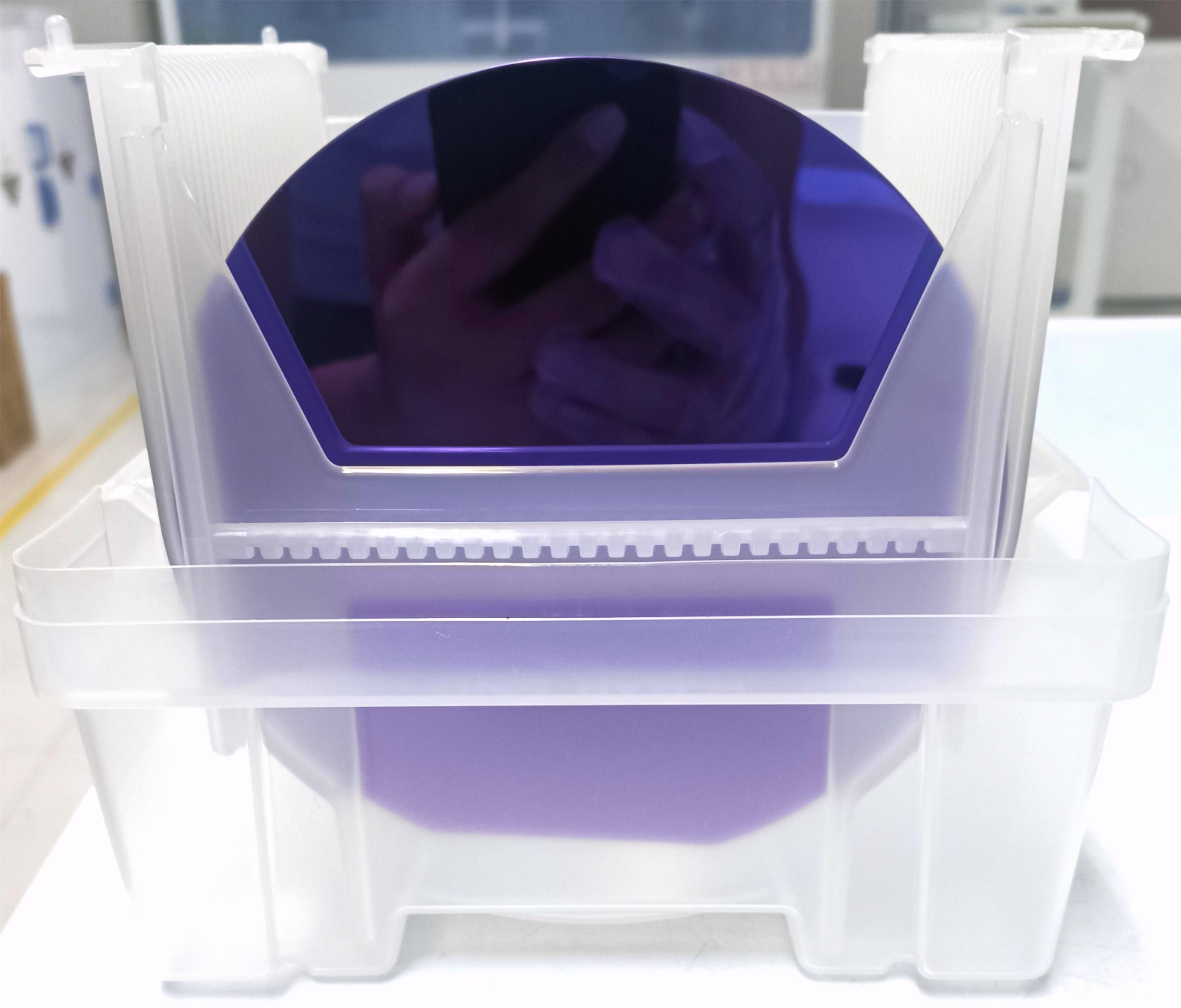
OMedaSemi provides stock and custom processing of thermal oxide wafer . Our featured products are thin film thermal oxide wafer and thick film thermal oxide wafer . Our thickest thermal oxide sheet is 15um, and the thinnest is 50nm.
SIZE:4inch 6inch 8inch
Thickness of Oxide Layer :50nm-15um
General deposit Method:LPCVD Furnace Wet Oxidation(100pcs/Chamber 50Pcs/Chamber 25Pcs/Chamber)
Lead Time:7days
Application:PIC,MEMS,SAW
Substrate:Clients can specify the silicon wafer ,and we do the oxidation process
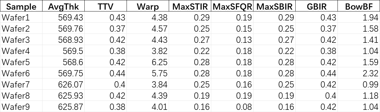
Our Innovation :Ultra-Flat-thermal Oxide-Wafer-TTV<500nmm
Also we have capbllity to fabricate the TTV<500nm silicon wafer in 6inch size,if you can interested in them ,we can fabricated ultra flat 8inch thermal oxide silicon wafer for you
Our stock
6 inches
Low resistivity 1-100 resistivity
1um thermal oxide wafer
2um thermal oxide wafer
3um thermal oxide wafer (SICOI SINOI)
8um thermal oxide wafer
10um thermal oxide wafer
15um thermal oxide wafer (applied to silicon nitride optical waveguide gyroscope, ultra-high aspect ratio thin film low loss optical waveguide)
High resistance thermal oxide wafer (>10000 Oh*m)
4.7um thermal oxide wafer (LNOI LTOI and other electro-optic modulators)
8 inches
High resistance thermal oxide wafer (>10000 Oh*m)
4.7um thermal oxide sheet (LNOI LTOI and other electro-optic modulators)
8.2um thermal oxide sheet (LNOI LTOI and other electro-optic modulators)
Customized Thermal Oxide Wafer
At the same time, we can also provide low-cost and fast customized thermal oxide wafer services,4inch 6-inch 8-inch equipment, 100 wafers per furnace, high efficiency and low cost
OMeda (Shanghai Omedasemi Co.,Ltd) was founded in 2021 by 3 doctors with more than 10 years of experience in nanpfabrication. It currently has 15 employees and has rich experience in nanofabrication (coating, lithography, etching, two-photon printing, bonding) and other processes. We support nanofabrication of 4/6/8-inch wafers.