OMedaSemi Provide advanced PZT thin Film Film for electro optical Modulator and Piezoelectric Device
For Electro Optical Modulator Application
Data we provide:Refractive Index and Absorption Data For Photonics integrated Circuit
PZTOI( Lead Zirconate Titanate On insulator)Wafer is a material with a super strong electro-optical effect, and its electro-optical coefficient is 6 times that of LiNbO3. At the same time, PZT has nonlinear effect, acousto-optic effect, and piezoelectric effect.
Comparison of PZT/BTO/LN/SI
| Material | Electro-optic coefficient (pm/V) | Intrinsic bandwidth (GHz) | Light transmission range (nm) | Refractive index | Operating temperature |
| PLZT | 200 | >200 | >500 | 2.4 | <600℃ |
| LN | 30 | >200 | >330 | 2.2 | |
| BTO | 1000 | 70 | >430 | 2.3 | <120℃ |
| Si | - | 50 | >1200 | 3.4 |
* All the "electro-optic coefficients" in the table are measured values in the electro-optic modulator
* The relationship between the modulator drive voltage Vπ, power consumption P and electro-optic coefficient r: Vπ ∝ 1/r, P ∝ 1/ r2
* PZT has a large light transmission range and can be used in AR/VR and visible light radar, which is impossible with silicon
If you are interested in this material ,and want to know its application, please see the following paper,After you see all the paper and you will know which kind of wafer do you need and which application you can do :
 PZT photonic materials and devices platform.pdf
Light Modulation in Silicon Photonics by PZT Actuated Acoustic Waves.pdf
Photonic integration based on a ferroelectric thin film platform.pdf
Integrated electro-optic modulator on lead zirconate.pdf
Highly efficient lead zirconate titanate ring modulator.pdf
Broadband PZT electro-optic modulator.pdf
200 GBd Electro-optic PLZT Modulator.pdf
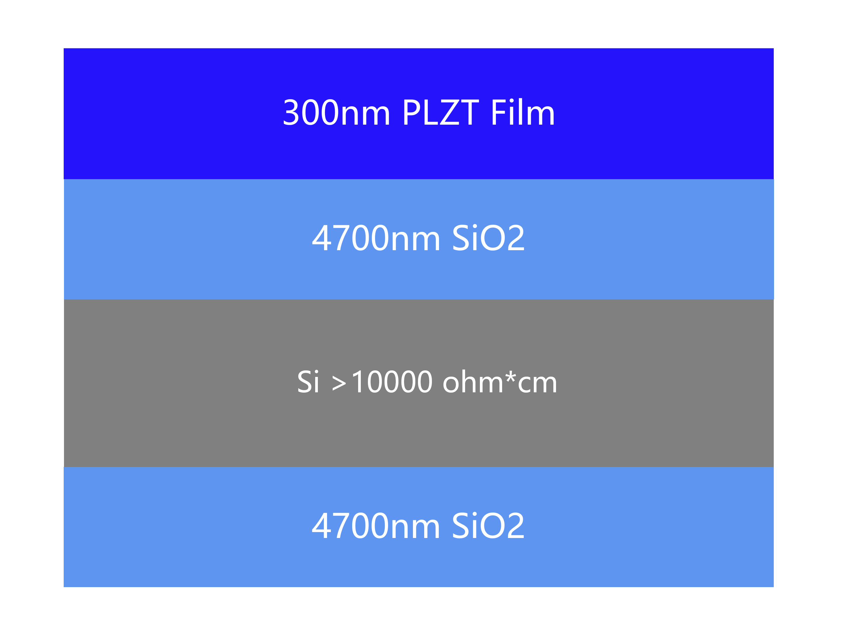
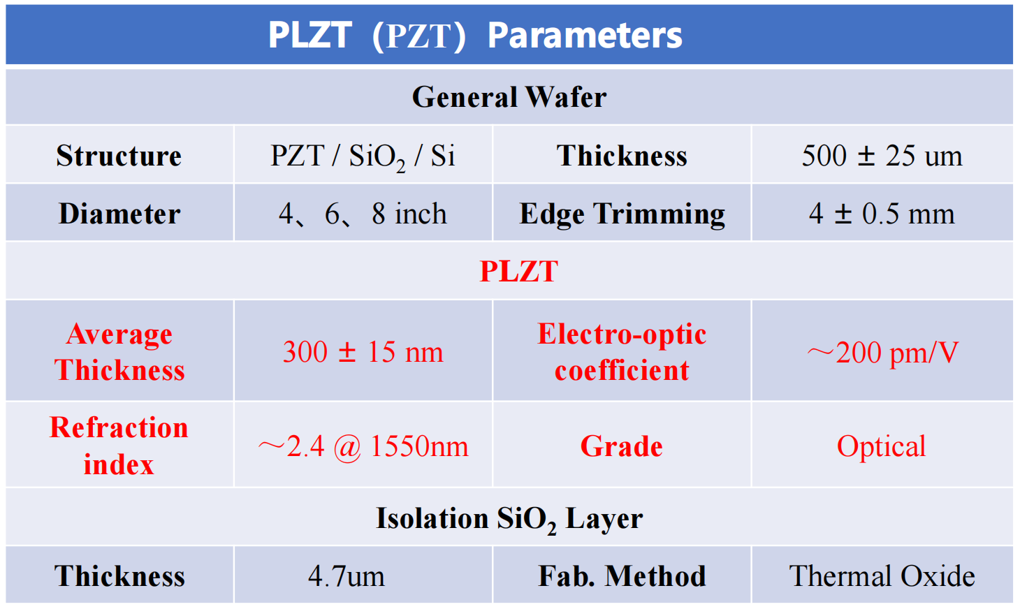
*Specification
For Piezoelectric Device
Single Crystal PZT thin film show extremely strong piezoelectric/inverse piezoelectric effects, with piezoelectric coefficients ranging from d31 to 180 pm/V and d33 to 400 pm/V.
The material exhibits extremely high stability, with a heat resistance temperature reaching 600 ºC, far exceeding that of existing piezoelectric functional ceramics.
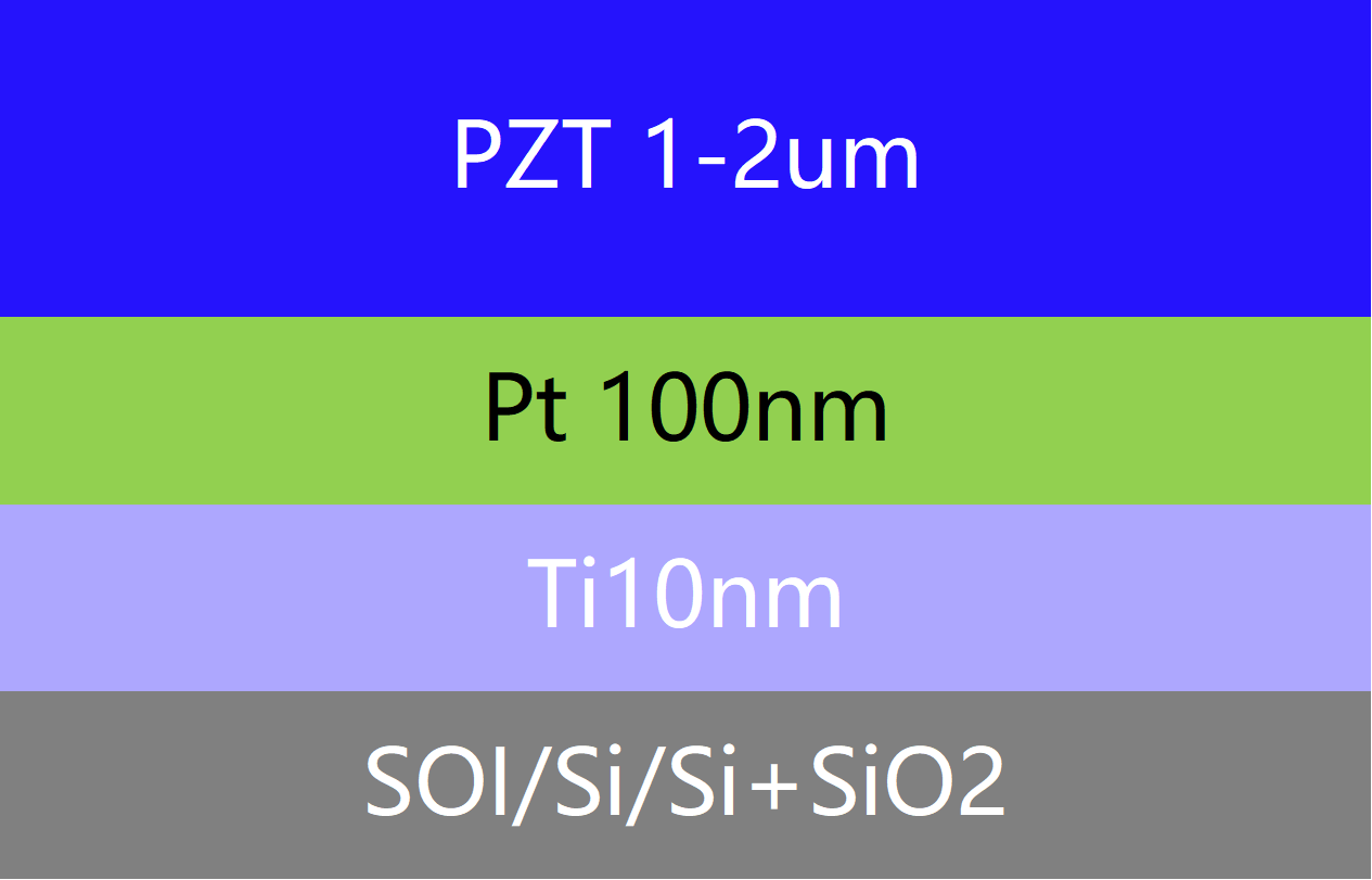
1-2 μm thick SCP single crystal thin film is grown on silicon substrates, is compatible with semiconductor processes, and is suitable for mass production of MEMS chips.
Comparison:
| Material | Piezoelectric coefficient d31 (pm/V) | polarization process | Curie temperature (°C) | Dielectric constant |
| SCPZT piezoelectric single crystal | 180 | unnecessary | 600 | ~300 |
| Polycrystalline PZT | ~150 | High temperature and high pressure polarization | <400 | 2000 |
| ALN | 10 | unnecessary | - | 10 |
| AlScN | 45 | unnecessary | - | 15 |
* Application :
electro-optic modulators
optical switches
optical gyroscopes
acousto-optic devices
optical MEMS
* Provide device etching foundry
*Provide polarization foundry or a complete set of polarization equipment and processes Provide optoelectronic chip design services
*Photolithography → Etching → Liftoff Electrode
*The processed modulator can obtain the strongest electro-optic effect after DC electric field polarization (electro-optic coefficient ~200 pm/V)
OMeda (Shanghai Omedasemi Co.,Ltd) was founded in 2021 by 3 doctors with more than 10 years of experience in nanpfabrication. It currently has 15 employees and has rich experience in nanofabrication (coating, lithography, etching, two-photon printing, bonding) and other processes. We support nanofabrication of 4/6/8-inch wafers.
