Practical Article - Comparison of Several Exposure Methods
Today, we're sharing an article comparing the accuracy, size, and cost of several commonly used exposure methods. After reading this article, you'll be able to choose the most cost-effective exposure method based on your needs.
This article discusses five exposure methods: contact exposure, stepper exposure, laser direct writing, electron beam lithography, and nanoimprint lithography (we'll also consider nanoimprint lithography as one of the exposure methods in this article).
Mask-Based Lithography
Mask-Based Lithography mainly consists of two types: contact lithography and stepper lithography.
Features of Contact Lithography
1. Suitable for processing line widths; processing patterns with line widths greater than 2µm.
2. The mask and pattern size are 1:1. If you want a 3µm line width pattern, you need a mask with 3µm line width.
3. Because it's a contact exposure method, the area of a single pattern can be arbitrarily large (importantly, it cannot be larger than the wafer).
4. Commonly used for processing micro-nanostructures with line widths greater than 2µm. Front-side alignment accuracy: ≤0.5µm, back-side alignment accuracy: ≤1µm.
5. Supports exposure of small wafers.
6. Direct write is generally preferred for processing small areas, but contact lithography can be used for larger samples.
7. Conclusion: Contact lithography is required when line widths are greater than 2µm, multiple samples are required, or the layout area is large.
Related Equipment Accuracy Introduction:
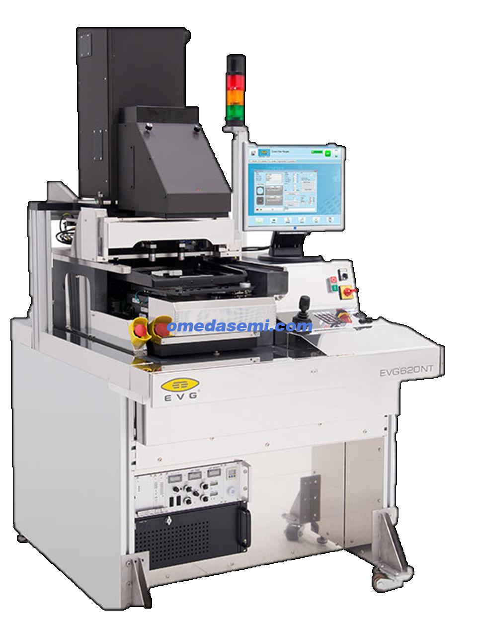
Equipment Name: Double-Sided Alignment Lithography System
Brand Model: EVG 620NT
Specifications
• Substrate Size: Fragment/2/4/6 inches
• Supports double-sided alignment and bonding alignment
• Minimum Linewidth: 0.8 μm
• Light Intensity Uniformity: ≤3%
• Front-Side Alignment Accuracy: ≤0.5 μm
• Back-Side Alignment Accuracy: ≤1 μm Micro-Nanostructure and Device Patterning Lithography
Stepper Lithography Features
Currently used equipment: Canon 3030 6-inch, ASML 4-inch, and 8-inch
1. Suitable for processing linewidth range: 2μm-130nm
2. Acceptable substrate: 468-inch substrate. However, it should be noted that DUV has relatively high substrate requirements. For example, the Canon 6-inch DUV system we use requires a substrate.
A: Chamfer C > 0.2
B: TTV < 5μm, BOW < 20μm WRAP < 20µm
C: Flat edge 57.5mm
D. Maximum thickness supported is 800µm
3. Unlike contact lithography, stepper lithography equipment exposes the entire surface. Contact lithography exposes the entire surface in one pass, while stepper lithography exposes regions. The maximum area per exposure, also known as the maximum write field, is 20×20mm. This means the maximum pattern size for a single chip cannot exceed this size. If it exceeds this size, multiple masks will be required for panelization. For example, if your pattern size is 20-30mm, you will need two masks; 40-40mm will require four masks; and 50-50mm will require nine panels.
4. The scaling ratio is 5:1. If you want to create a 200nm linewidth pattern, you will need a 1µm linewidth mask. This scaling ratio makes stepper panels so affordable.
5. Masks can be prepared using two methods: laser direct writing and electron beam lithography. Electron beam lithography produces masks with better linewidth accuracy, and the resulting pattern linewidth precision is also more accurate. However, masks made using electron beam lithography are significantly more expensive than those produced using laser direct writing.
6. Conclusion: When linewidths are less than 150nm (our company's minimum linewidth is 150nm) and large areas or multiple samples are required, stepper lithography is the preferred method.
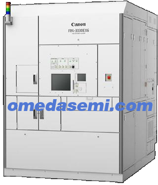
Equipment Name: Stepper Lithography Machine
Brand and Model: CANON FPA-3030EX6
Specifications
• Substrate Size: 4/6 inch
• Minimum Line Width: 150 nm
• Mask Scale Ratio: 5:1
• Alignment Accuracy: ≤40 nm
• Focus Accuracy: ≤100 nm
• Step Accuracy: ≤20 nm
Main Function: Micro-nanostructure and device patterning lithography
Maskless Lithography
Maskless lithography has two types: laser direct writing and electron beam lithography.
Laser Direct Writing Features
1. Processable Line Width Range; Patterns with Line Widths Greater than 500 nm
2. Capable of processing small wafers
3. Because maskless lithography is a process involving maskless lithography, the processing cost is related to the area of the pattern being processed. The larger the pattern area, the higher the price.
4. Maskless lithography has low throughput and a poor cost-performance ratio. However, due to the lack of small-linewidth lithography machines in China and the high initial investment in mask exposure reticles, laser direct writing is often used for proofing during trial production and process verification.
5. Conclusion: When linewidths are greater than 500nm and the processing area is small, laser direct writing is required.
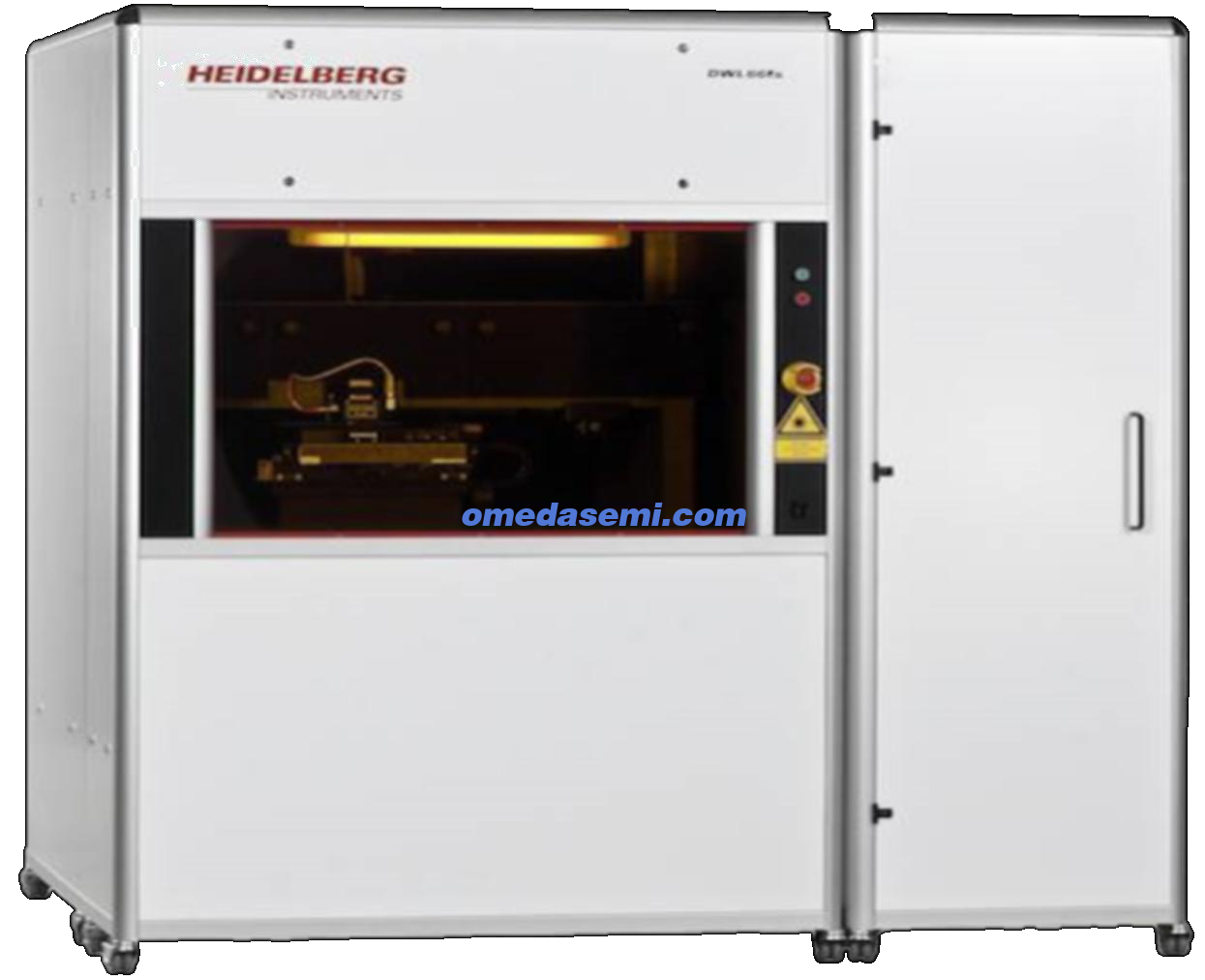
Equipment Name: Laser Direct Writing System
Brand Model: Heidelberg Instruments DWL66+
Specifications
• Minimum Feature Size: 300 nm
• Grid Grid: 7 nm
• Linewidth Bevel Roughness: 50 nm
• Linewidth Uniformity: 60 nm
• Overlay Accuracy: ≤ 100 nm
• Photolithography Speed: 3 mm²/min
Main Function: Micro-nanostructure and Device Patterning
Electron Beam Lithography Features
1. Processable Linewidth Range: Patterns with linewidths greater than 50 nm (with repeated adjustments, widths below 30 nm are also possible)
2. Capable of processing small wafers. Currently, there are two main types of equipment: Raith and Jeol. Raith supports any size, while Jeol's high-precision technology currently only supports small wafer sizes: 1 cm square, 2 cm square, 1 inch round, 2 inch round, 4 inch round, and 6 inch round. The maximum thickness supported is 6.35 mm.
3. Because it's maskless lithography, processing costs are related to the area of the pattern being processed; larger patterns increase the price.
4. Electron-beam lithography has low throughput, but it can produce high-precision structures. Limited by the lack of high-precision UV lithography equipment in China, electron-beam lithography is a powerful tool for scientific research and corporate R&D. Currently, many masks and marks used in high-precision lithography products are produced using electron-beam lithography. In the long term, electron-beam lithography will play a key role in small-linewidth tapeouts.
5. Conclusion: When the linewidth is less than 150nm, electron beam is generally the right choice. When the linewidth is less than 500nm and the area is less than 3mm-3mm, electron beam is generally the right choice. Generally speaking, electron beam is suitable for high-precision, small-size, and small-pattern exposure.
Processing Capabilities:
Exposure Linewidth Accuracy:
>200nm: ±5%,
<=200nm: ±10nm
Supported Electron Beam Photoresists: PMMA, HSQ, ZEP
Positive Resists: ZEP 520, PMMA A4/A10, AR-P 6200
Negative Resins: MA-N, HSQ Fox14, and our own thin negative resists
Equipment Model 1: JEOL JBX-9500FS
Processing Accuracy:
Accelerating Voltage: 100kV
Exposure Resolution: 10nm
Overlay Accuracy: 10nm
Field Stitching Accuracy: 10nm
Writing Field Size: 1mm*1mm
Scanning Frequency: 100MHz
Acceptable Substrate Sizes: 1cm*1cm, 2cm*2cm, 2-inch, 3-inch, 4-inch, 6-inch
OMeda (Shanghai Omedasemi Co.,Ltd) was founded in 2021 by 3 doctors with more than 10 years of experience in nanpfabrication. It currently has 15 employees and has rich experience in nanofabrication (coating, lithography, etching, two-photon printing, bonding) and other processes. We support nanofabrication of 4/6/8-inch wafers.