Paper Download

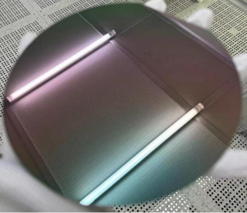
OMedaSemi can provide ultra low loss silicon nitride wafer , we use LPCVD/PECVD method to deposite Silicon Nitride film on thermal oxide wafer ,the film have good quality ,loss of thin film is 1dB/M,also the max size is 6 inch ,the max thickness is 800nm,we also have many stock ,you can visit this page to know more : Ultra Low Loss Silicon Nitride Thin Film Wafer

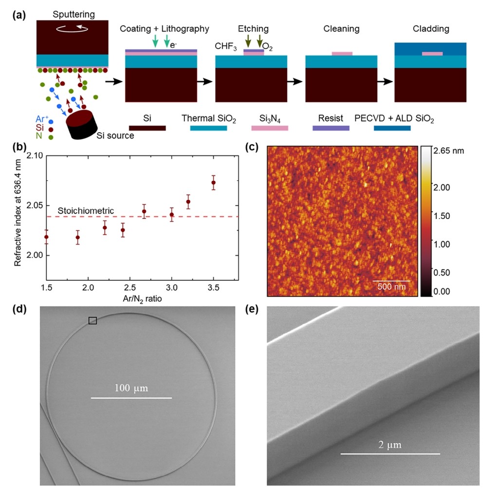
The article "Low-Temperature Sputtered Ultralow-Loss Silicon Nitride for Hybrid Photonic Integration" presents the development of a process to fabricate ultra-low-loss silicon nitride (Si₃N₄) photonic devices using reactive sputtering at room temperature. This method offers a CMOS-compatible process for integrating Si₃N₄ with other materials without requiring high-temperature annealing. Key highlights include:

1. **Room-Temperature Sputtering Process**: Si₃N₄ films are deposited at room temperature using reactive sputtering, avoiding the formation of lossy hydrogen bonds. This results in an initial propagation loss of 32 dB/m without thermal annealing.
2. **Improved Optical Performance with Annealing**: After a 400°C annealing process, the propagation loss decreases significantly to 5.4 dB/m, with the intrinsic quality factor (Q) of resonators reaching 6.2 million. Further annealing at 800°C reduces the loss to 3.5 dB/m, with Q-factors exceeding 10 million.
3. **Soliton Frequency Comb Generation**: The low-loss resonators enabled the generation of Kerr soliton frequency combs with threshold powers as low as 1.1 mW. These combs were generated at both 1.3 µm and 1.5 µm wavelengths, demonstrating the technology's potential for nonlinear photonic applications.
4. **Applications**: This low-temperature process is compatible with hybrid photonic integration, enabling applications in telecommunications, optical communication, nonlinear optics, and quantum computing. It offers significant advancements in integrating Si₃N₄ with silicon electronics, lithium niobate, and other materials.
In conclusion, the article highlights the scalability and versatility of sputtered Si₃N₄ for future high-performance photonic integrated circuits (PICs), expanding its potential applications in various fields【23†source】.
OMeda (Shanghai Omedasemi Co.,Ltd) was founded in 2021 by 3 doctors with more than 10 years of experience in nanpfabrication. It currently has 15 employees and has rich experience in nanofabrication (coating, lithography, etching, two-photon printing, bonding) and other processes. We support nanofabrication of 4/6/8-inch wafers.