Paper Download
OMedaSemi develop 4-6 inch SICOI wafers (silicon carbide on insulator wafers). The wafers use Direct Bonding(hydropholic bonding) or surface activated bonding technology to bond thermal oxide wafers and 4H high-purity semi-insulating silicon carbide wafers together, and then control the thickness to the thickness you need through ion implantation, annealing, thinning or direct thinning and CMP polishing. It is worth noting that ion implantation and direct CMP and thinning have their own advantages and disadvantages.we also have many stock ,you can visit this page to know more :6inch 4H HPSI SICOI Wafer
The article explores the photoluminescence properties of ion-implanted Er³⁺-defects in thin-film 4H-Silicon-Carbide-On-Insulator (4H-SiCOI) and its potential for integrated quantum photonics applications. It investigates the properties of Er³⁺ defects, focusing on their photoluminescence, optical lifetime, and polarization characteristics.
Key points include:
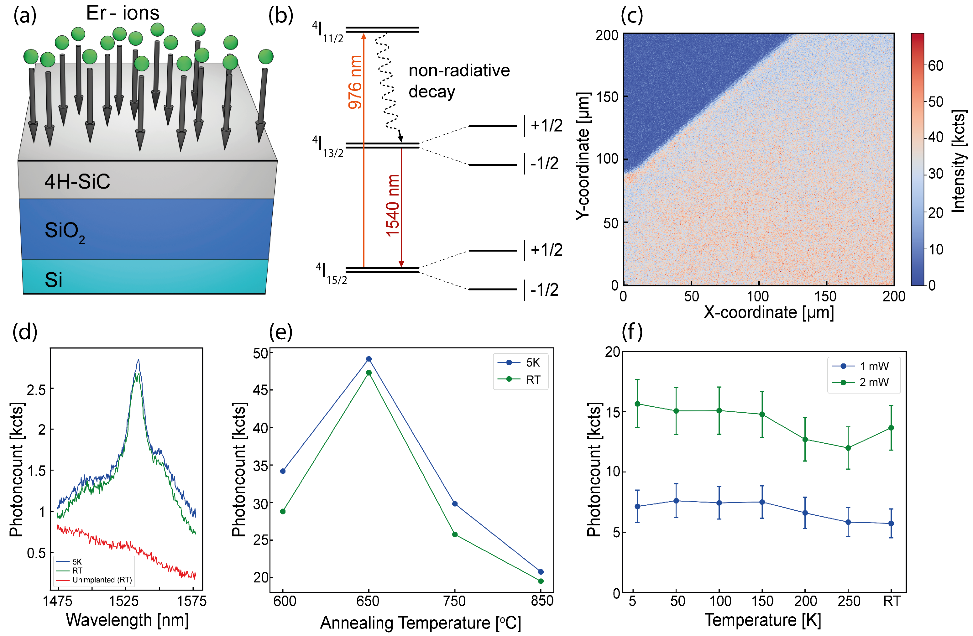
Er³⁺ in 4H-SiCOI: The study discusses how erbium (Er³⁺) defects, embedded in 4H-SiCOI through ion implantation, are promising candidates for use in quantum technologies due to their ability to function as single-photon emitters in the telecommunications band.
Material Benefits: 4H-SiCOI provides a scalable platform for quantum photonics with features like a wide bandgap (3.26 eV) that helps reduce the quenching of Er³⁺ photoluminescence at higher temperatures, making it suitable for integrated quantum systems.
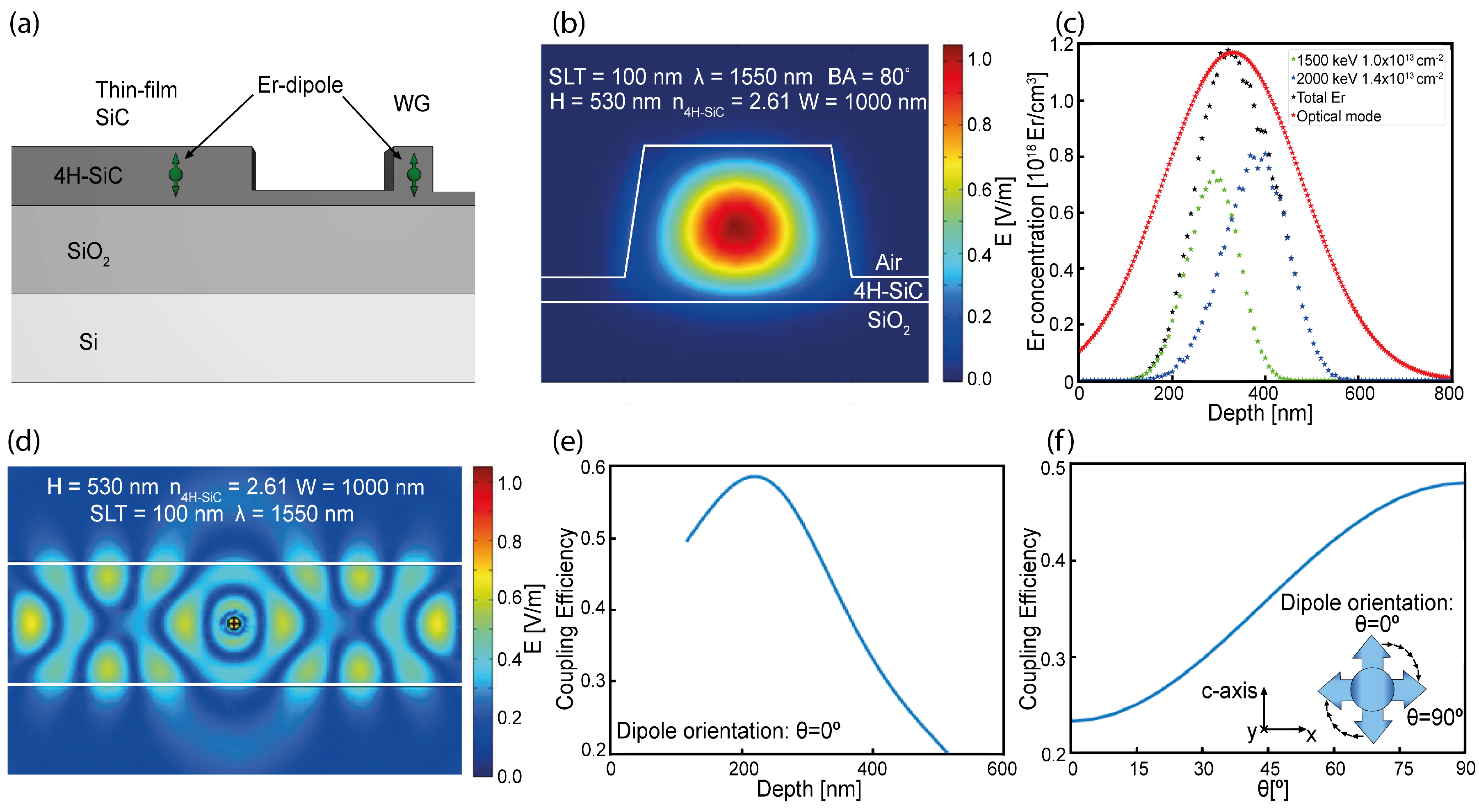
Ion Implantation & Waveguide Coupling: The paper describes the processes used for ion implantation and the coupling of Er³⁺ defects to waveguides in photonic circuits. The efficiency of coupling the defects to the optical mode of the waveguide is studied.
Optical Lifetime and Polarization: The study investigates the optical lifetime of the Er³⁺ defects and the temperature dependence of these lifetimes, concluding that the defects can be stable at different temperatures. The polarization properties of the Er³⁺ defects are also analyzed, revealing the presence of a C3V-symmetry.
Future Potential: The paper suggests that the defects could be useful in quantum communication and computing applications, including quantum memory and gate operations. The findings could lead to improved designs for quantum photonic systems, such as integrated photon pair sources for quantum storage.
Conclusion and Outlook: The research presents 4H-SiCOI as a strong material for integrated quantum photonics, with potential applications in scalable quantum memory and communication systems. The study also points to future directions in improving the understanding and use of such materials in quantum technologies.
This research provides valuable insights into the properties of Er³⁺ defects for their integration into quantum photonic systems, opening up possibilities for future developments in quantum communication and memory technologies.
OMeda (Shanghai Omedasemi Co.,Ltd) was founded in 2021 by 3 doctors with more than 10 years of experience in nanpfabrication. It currently has 15 employees and has rich experience in nanofabrication (coating, lithography, etching, two-photon printing, bonding) and other processes. We support nanofabrication of 4/6/8-inch wafers.
