Paper Download
 Integrated Lithium Niobate Photonic Millimeter-Wave Radar.pdf
LNOI Wafer OMedaSemi can provide 4-inch and 8-inch LNOI wafers and LN-SOI We provide 4-8 inch LNOI wafers (thin-film lithium niobate), which use surface activated bonding technology to bond thermal oxide wafers and X-lithium niobate crystal wafers together, and then control the thickness to the thickness you need through ion implantation, annealing, thinning or direct thinning and CMP polishing. It is worth noting that ion implantation and direct CMP and thinning have their own advantages and disadvantages. We provide customers with a variety of LNOI products. Also we are developing 6inch LTOI(lithium tantalate) wafer.We also have a large stock available. You can visit this page to learn more:https://en.omedasemi.com/linbo3_on_insulator.html
his article introduces a novel integrated lithium niobate (TFLN)-based photonic millimetre-wave radar, addressing key challenges in achieving high-resolution radar sensing for the upcoming 6G era. Unlike conventional photonic radars, which often rely on bulky discrete components, this radar is based on a compact, wafer-scale TFLN photonic chip, capable of generating broadband radar waveforms and processing received echoes with high efficiency.
The radar operates in the mmWave V band (40–50 GHz) and achieves impressive results such as multi-target ranging with a resolution of 1.50 cm, velocity measurement with a resolution of 0.067 m/s, and inverse synthetic aperture radar (ISAR) imaging with 1.50 cm × 1.06 cm two-dimensional resolution.
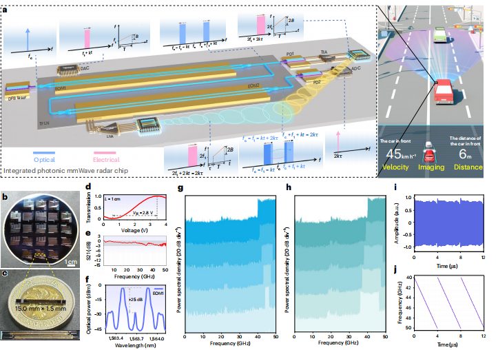
TFLN Electro-Optic Modulators (EOMs):
The first modulator generates radar waveforms via optical frequency multiplication.
The second modulator processes received echo signals using a frequency de-chirp technique, minimizing digital-to-analog and analog-to-digital converter bandwidth requirements.
High Performance:
The chip provides a scalable, compact solution for future high-resolution sensing applications, suitable for vehicle radar, airborne radar, and smart home technologies.
Its compactness and cost-effectiveness make it an ideal candidate for integration in future radar systems.
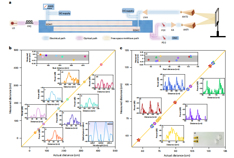
Resolution and Range: The radar achieves centimetre-level resolution and accurate distance measurements, even for small and weak targets, with no side-lobe interference greater than 6.5 dB.
Velocity Detection: The radar shows high accuracy in velocity detection, even for small Doppler shifts as low as 0.056 m/s, with an estimated maximum unambiguous velocity of 833 m/s.
Adaptive Cruise Control: High-resolution distance and velocity detection for enhanced safety in automotive systems.
Sensing and Imaging: The radar's ISAR imaging capabilities enable detailed imaging of various objects, such as airplanes and dolls, at high resolutions.
The integration of TFLN-based radar technology sets the foundation for compact, cost-effective, and high-performance radar systems, marking a significant step toward the 6G era. The work highlights the potential of integrated photonics to revolutionize radar systems, offering superior bandwidth, frequency agility, and low power consumption.
OMeda (Shanghai Omedasemi Co.,Ltd) was founded in 2021 by 3 doctors with more than 10 years of experience in nanpfabrication. It currently has 15 employees and has rich experience in nanofabrication (coating, lithography, etching, two-photon printing, bonding) and other processes. We support nanofabrication of 4/6/8-inch wafers.