Shanghai OMeda Micro provides X, Y, and Z-cut acoustic and optical grade lithium niobate crystals. It also processes lithium niobate wafers into LNOI thin-film lithium niobate wafers for photonic integrated circuits and surface acoustic wave devices.
 Research on the Fabrication of X-Cut Near-Stoichiometric Lithium Niobate Wafers.pdf
This study investigates the fabrication of X-cut near-stoichiometric lithium niobate (NSLN) wafers using the diffusion method. The research focuses on eliminating parasitic microdomains, optimizing the lithium diffusion process, and enhancing the electro-optical properties of NSLN wafers.
Fabrication Method
The diffusion method is employed to introduce lithium ions into congruent lithium niobate (CLN) wafers, creating NSLN.
Various Li-rich polycrystalline materials with different Li/Nb ratios (58/42, 56/44, 54/46) were synthesized to study their effect on diffusion.
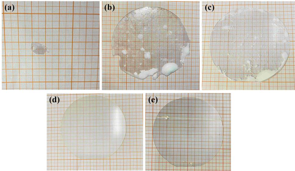
The optimal diffusion temperature was found to be 1180°C, ensuring high-quality wafers without cracks or twins.
Material Characterization
XRD analysis confirmed the presence of (Li₀.₉₄₁Nb₀.₀₅₉)Nb₀.₉₅₂₈O₃ and Li₃NbO₄ phases in the Li-rich polycrystalline material.
With increasing lithium content, the lattice parameters a and c decreased, indicating a structural change toward stoichiometry.
Microdomain Elimination & Electro-Optical Performance
A liquid electrode polarization method was designed to eliminate microdomains and achieve a single-domain state.
The piezoelectric coefficient (d₃₃) increased by 12% compared to CLN, demonstrating improved electro-mechanical properties.
The coercive field of NSLN wafers was significantly lower than that of CLN, facilitating ferroelectric domain engineering.
Physical and Optical Properties
The Curie temperature of NSLN reached 1198°C, higher than CLN, indicating enhanced thermal stability.
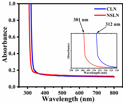
The UV absorption spectrum of NSLN exhibited a blue shift of 10 nm, making it more suitable for ultraviolet applications.
The refractive index of NSLN was higher and more uniform than that of CLN, benefiting optical device fabrication.
This research demonstrates that the diffusion method is a viable approach for fabricating high-quality X-cut NSLN wafers with enhanced electro-optical properties. The improved piezoelectric response, lower coercive field, and superior optical uniformity make NSLN wafers ideal for applications in integrated photonics, electro-optic modulators, and nonlinear optical devices.
OMeda (Shanghai Omedasemi Co.,Ltd) was founded in 2021 by 3 doctors with more than 10 years of experience in nanpfabrication. It currently has 15 employees and has rich experience in nanofabrication (coating, lithography, etching, two-photon printing, bonding) and other processes. We support nanofabrication of 4/6/8-inch wafers.