Paper Download
 Low-Temperature Direct Bonding of SiC to Si via Plasma Activation.pdf
We also have a large stock available. You can visit this page to learn more:https://en.omedasemi.com/composite-wafer.html
The paper discusses the low-temperature direct bonding of Silicon Carbide (SiC) to Silicon (Si) via plasma activation, specifically using O2 plasma. The primary focus is on optimizing the process parameters for high bonding efficiency and exploring the bonding mechanism. The authors use reactive ion etching (RIE) O2 plasma to activate the bonding surfaces and achieve an over 90% bonding efficiency. Key findings include:
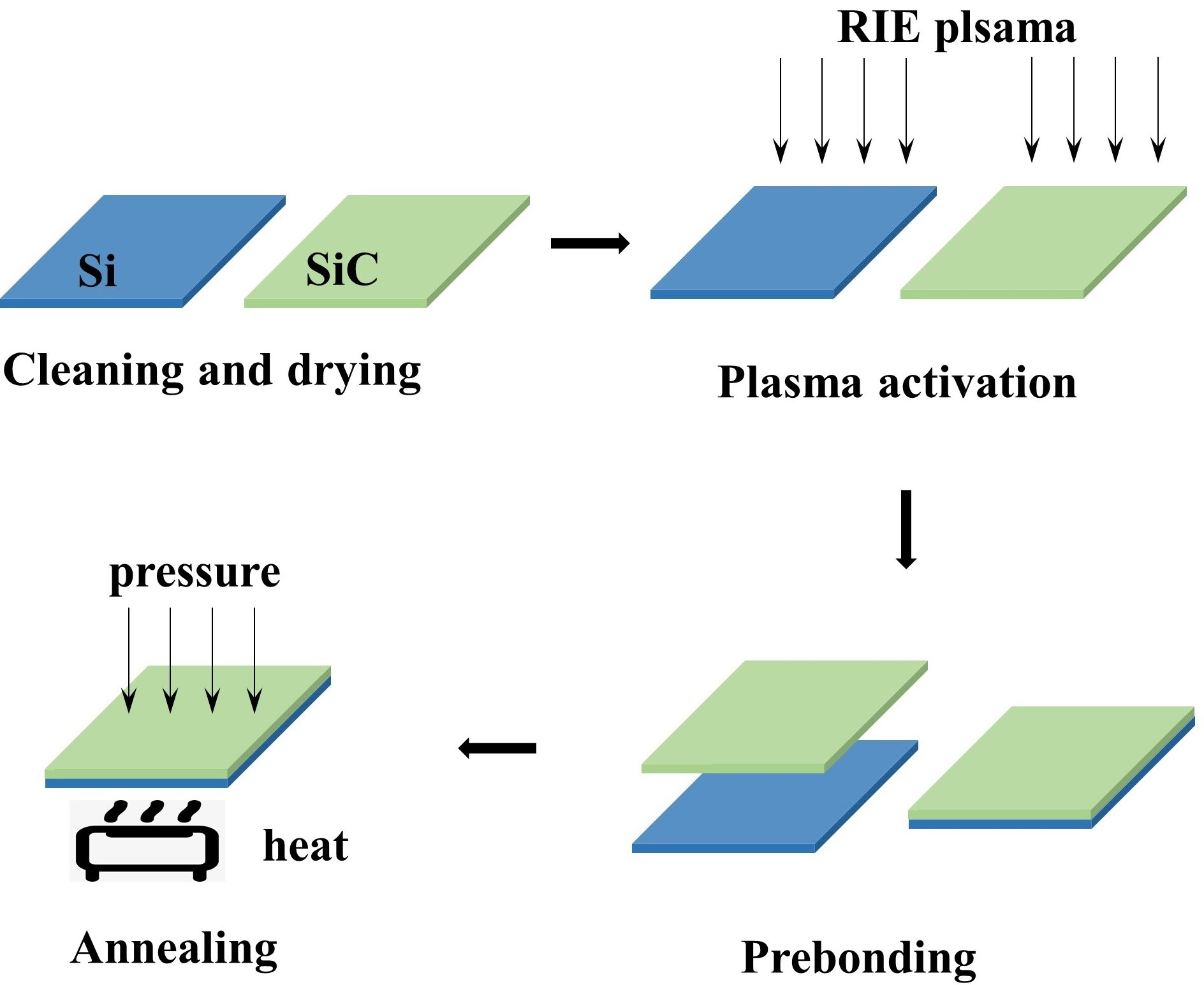
Plasma Activation and Bonding Efficiency: A 30-second plasma activation time was found to achieve the highest bonding efficiency, with diminishing returns at longer activation times.
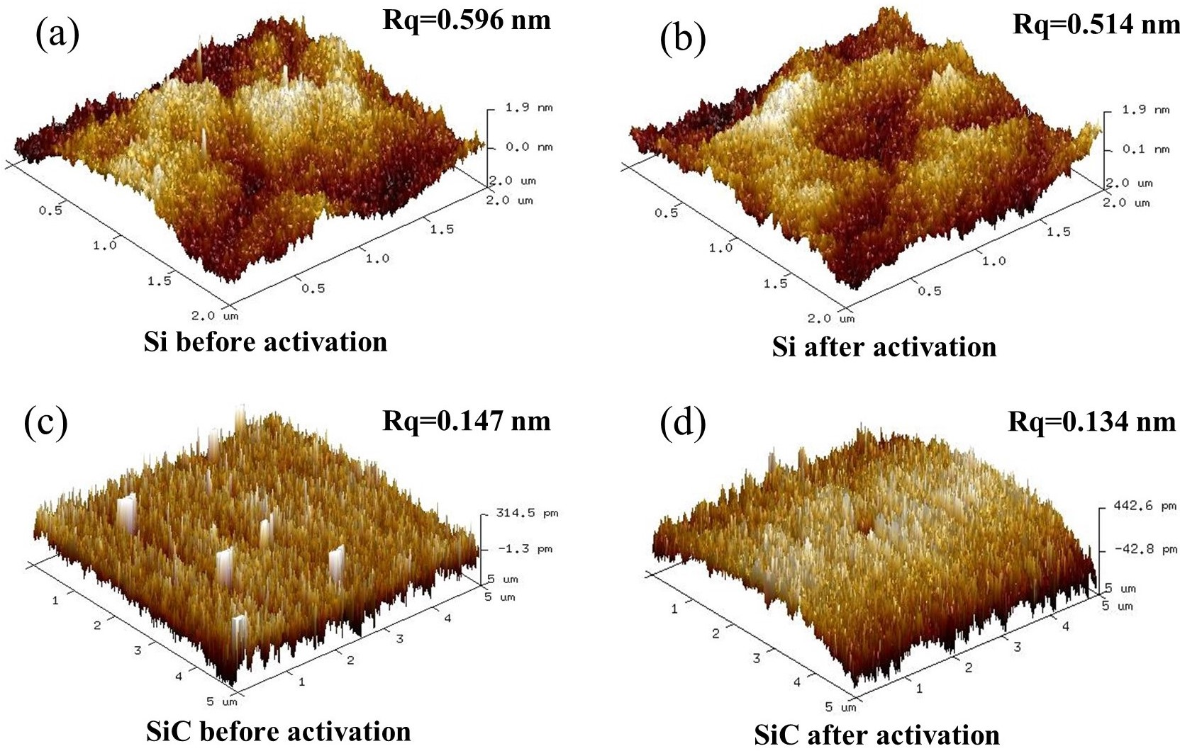
Surface and Interface Characterization: The study also investigates the surface roughness and chemical changes post-activation using atomic force microscopy (AFM) and X-ray photoelectron spectroscopy (XPS), revealing the oxidation of the surfaces. The surface roughness slightly decreases after plasma treatment, which improves the bonding.
Annealing and Amorphous Layer: Transmission electron microscopy (TEM) was used to observe the bonding interface, showing an amorphous oxide layer. Annealing at 300°C reduced the thickness of this layer, but it couldn’t be entirely eliminated at low temperatures.
Bonding Mechanism: The bonding process is detailed, showing how dangling bonds and water molecules interact at the interface to form stable covalent bonds. The presence of water molecules at the interface contributes to the bonding strength, but their elimination is crucial for improving bonding quality.
In conclusion, the paper demonstrates that while the bonding efficiency can exceed 90%, an amorphous oxide layer persists in the interface, limiting the electrical properties of the bonded SiC/Si structure. Higher annealing temperatures or better activation sources are needed to reduce this layer and improve performance.
OMeda (Shanghai Omedasemi Co.,Ltd) was founded in 2021 by 3 doctors with more than 10 years of experience in nanpfabrication. It currently has 15 employees and has rich experience in nanofabrication (coating, lithography, etching, two-photon printing, bonding) and other processes. We support nanofabrication of 4/6/8-inch wafers.