Paper Download

We also have a large stock available. You can visit this page to learn more:https://en.omedasemi.com/silicon_carbide_on_insulator_wafer.html
OMedaSemi develop 4-6 inch SICOI wafers (silicon carbide on insulator wafers). The wafers use Direct Bonding(hydropholic bonding) or surface activated bonding technology to bond thermal oxide wafers and 4H high-purity semi-insulating silicon carbide wafers together, and then control the thickness to the thickness you need through ion implantation, annealing, thinning or direct thinning and CMP polishing. It is worth noting that ion implantation and direct CMP and thinning have their own advantages and disadvantages.

This article discusses the development of low-dissipation nanomechanical devices fabricated from monocrystalline 4H-silicon carbide (SiC), aiming to overcome the challenges of internal material damping in nanomechanical resonators. These resonators are essential for applications in sensing, timing, and quantum systems. The authors present a method of fabricating these resonators from bulk 4H-SiC, achieving ultra-low dissipation rates— as low as 2.7 mHz— which is an order of magnitude lower than previous SiC devices. This results in a high quality factor (Q) of 20 million at room temperature, setting a new standard for SiC resonators.
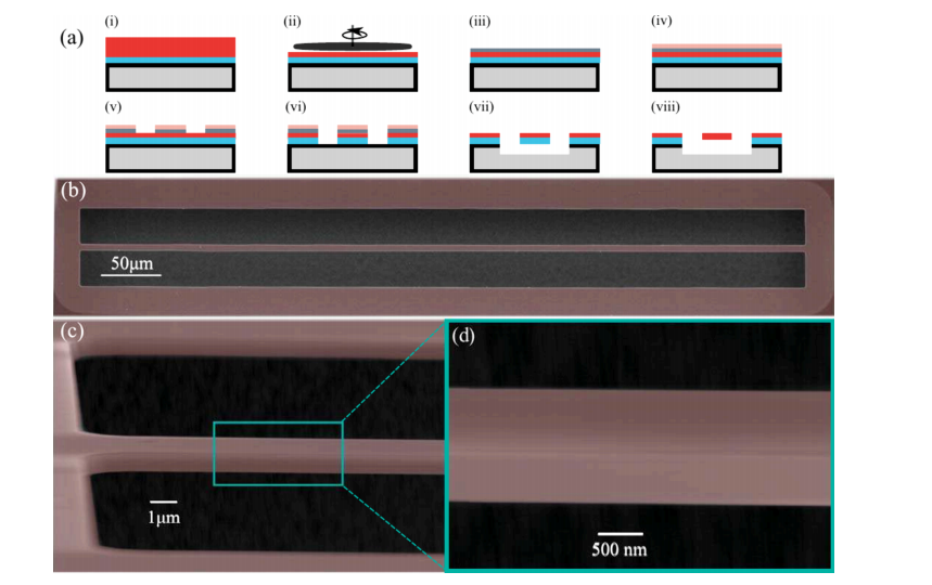
The fabrication process involves using bulk sublimation-grown 4H-SiC crystals, followed by a grind-and-polish technique to create defect-free thin films, minimizing internal damping. The devices showed significant improvements in terms of mechanical dissipation, with dissipation rates lower than previous reports in both crystalline SiC and high-stress amorphous SiC resonators. These low-dissipation characteristics enable the observation of nonlinear dissipation in SiC nanomechanical resonators, which is crucial for applications such as mass sensing and nanomechanical computing.
The authors also compare their results with other materials, demonstrating that 4H-SiC resonates with much lower dissipation than its 3C-SiC and amorphous SiC counterparts, offering substantial advantages for high-performance nanomechanical devices. This work opens the door to using SiC for more sensitive and reliable resonators in a range of technologies, including inertial sensing, quantum computing, and optomechanics.
OMeda (Shanghai Omedasemi Co.,Ltd) was founded in 2021 by 3 doctors with more than 10 years of experience in nanpfabrication. It currently has 15 employees and has rich experience in nanofabrication (coating, lithography, etching, two-photon printing, bonding) and other processes. We support nanofabrication of 4/6/8-inch wafers.