Paper Download
OMedaSemi develop 4-6 inch SICOI wafers (silicon carbide on insulator wafers). The wafers use Direct Bonding(hydropholic bonding) or surface activated bonding technology to bond thermal oxide wafers and 4H high-purity semi-insulating silicon carbide wafers together, and then control the thickness to the thickness you need through ion implantation, annealing, thinning or direct thinning and CMP polishing. It is worth noting that ion implantation and direct CMP and thinning have their own advantages and disadvantages.
We also have a large stock available. You can visit this page to learn more:https://en.omedasemi.com/silicon_carbide_on_insulator_wafer.html
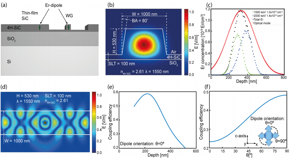
This article investigates the photoluminescence properties of erbium (Er³⁺) defects in 4H-silicon-carbide-on-insulator (4H-SiCOI) materials, a promising platform for integrated quantum photonics. The study focuses on enhancing the photoluminescence (PL) and photoluminescence excitation (PLE) characteristics of Er³⁺ defects through optimized ion implantation and thermal annealing processes.
The authors examine the key properties such as PL intensity, optical lifetime, and polarization of the Er³⁺ defects in thin-film 4H-SiCOI, revealing insights into their potential applications in quantum systems. A key finding is the temperature-independent intensity of the Er³⁺ emission, with minor changes in emission line shapes and widths at different temperatures, which suggests a robust performance for quantum communication applications. The study also reports the optical lifetime behavior and polarization properties of these defects, showing that Er³⁺ defects exhibit C3V symmetry.
Additionally, the study highlights the importance of optimizing implantation conditions and annealing processes to minimize defect-induced quenching and maximize the utility of Er³⁺ defects for integrated quantum devices. The research paves the way for further advancements in scalable, integrated quantum photonic systems using silicon carbide platforms, with particular focus on leveraging Er³⁺ defects for single-photon sources and quantum memory applications.
OMeda (Shanghai Omedasemi Co.,Ltd) was founded in 2021 by 3 doctors with more than 10 years of experience in nanpfabrication. It currently has 15 employees and has rich experience in nanofabrication (coating, lithography, etching, two-photon printing, bonding) and other processes. We support nanofabrication of 4/6/8-inch wafers.
