
Key points include:
Challenges with Non-native Substrates: The paper highlights the challenges posed by current non-native substrates (such as sapphire and silicon) used for GaN growth, which cause lattice mismatches leading to defects in GaN films.
QST® Technology: Qromis' QST® technology provides a thermal expansion match with GaN, facilitating the growth of thicker GaN layers on large diameter substrates. This makes it suitable for producing high-quality, freestanding GaN substrates.
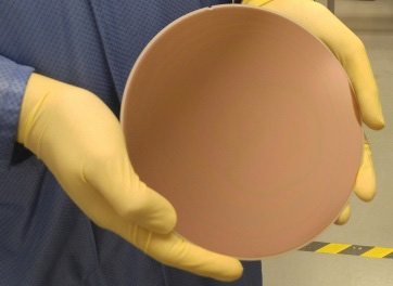
Manufacturing Process: The process involves growing GaN via HVPE on QST® substrates, followed by a seed removal technique that results in freestanding GaN crystals. The crystals are then subjected to wafering, grinding, cutting, and polishing to produce high-quality, epi-ready GaN substrates.
Characterization and Results: The GaN substrates produced show excellent structural quality, with defect densities significantly lower than those found in GaN films grown on non-native substrates. The curvature of the substrates also meets the standards needed for device manufacturing.
Cost Analysis and Commercial Potential: A cost analysis suggests that the manufacturing of 100 mm and 150 mm freestanding GaN substrates could be achieved at a cost of under $1,000 per wafer, with the potential to reduce costs further with higher volume production.
In conclusion, the paper presents a promising approach to the large-scale production of high-quality GaN substrates, which is essential for the continued growth and commercialization of GaN-based electronics.