This paper presents the development of an electrically pumped ultra-efficient quantum frequency conversion (QFC) chip on a thin film lithium niobate (TFLN) platform, aimed at enabling seamless interconnection between quantum systems operating at different wavelengths. The chip connects the telecom and visible bands and is based on a periodically poled lithium niobate (PPLN) microring resonator (MRR) with ultra-high normalized conversion efficiency.
Key points include:
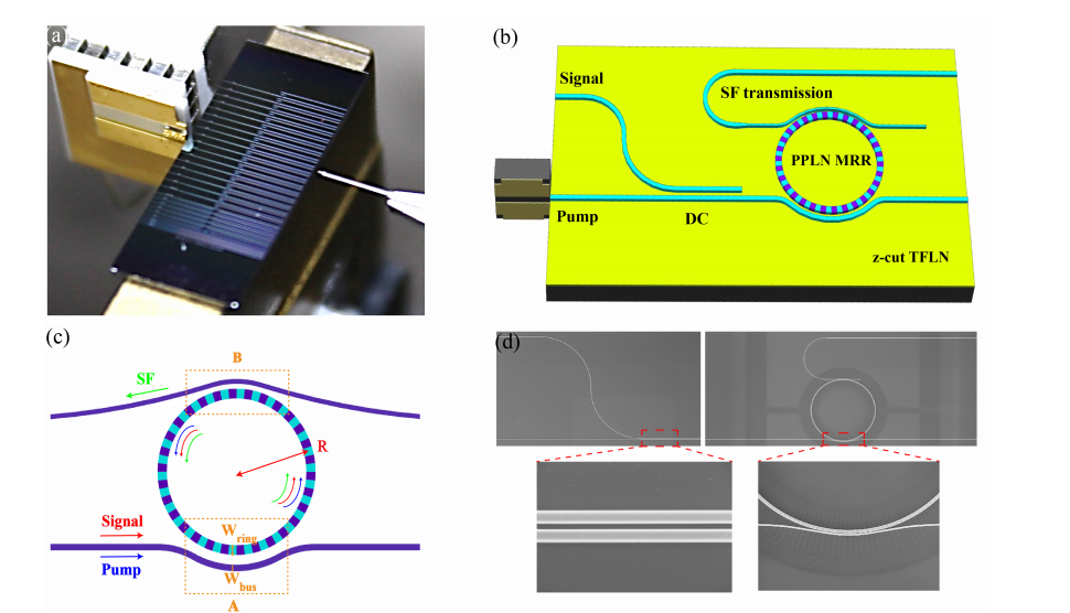
Hybrid Integration and Efficiency: The chip integrates a hybrid-distributed feedback (DFB) laser with a TFLN chip, achieving a normalized conversion efficiency of 386,000%/W and requiring an ultra-low pump power of just 360 µW, more than two orders of magnitude lower than traditional straight waveguide schemes.
Quantum Performance: The chip achieves an on-chip quantum efficiency (QE) of 57% and a noise count of approximately 7,000 counts per second, demonstrating efficient QFC at the single-photon level. This performance is achieved through the integration of a DFB laser with the TFLN photonic circuit using a butt-coupling technique.
Design and Fabrication: The QFC chip uses a double-pulley add-drop design for the MRR, enabling efficient coupling of signal, pump, and sum-frequency (SF) light, while minimizing noise and enhancing the conversion process. The microring resonator is optimized for triple resonance and high efficiency, with specific coupling parameters tailored for low pump power.
Low-Noise and Multi-Channel Capabilities: The design significantly reduces noise compared to previous PPLN-based QFC schemes, ensuring high-performance single-photon QFC. Furthermore, the chip is scalable and capable of supporting multiple channels, paving the way for multi-channel on-chip QFCs in future quantum networks.
Applications and Future Prospects: This electrically pumped, integrated QFC chip is a key advancement for quantum technologies, offering a scalable and efficient solution for connecting quantum systems across different wavelengths. It holds promise for integrated quantum optical systems, quantum communication, quantum computing, and quantum metrology.
In conclusion, this work demonstrates a breakthrough in chip-scale quantum frequency conversion, with the potential to significantly advance the development of quantum networks and integrated quantum optical systems.
OMeda (Shanghai Omedasemi Co.,Ltd) was founded in 2021 by 3 doctors with more than 10 years of experience in nanpfabrication. It currently has 15 employees and has rich experience in nanofabrication (coating, lithography, etching, two-photon printing, bonding) and other processes. We support nanofabrication of 4/6/8-inch wafers.