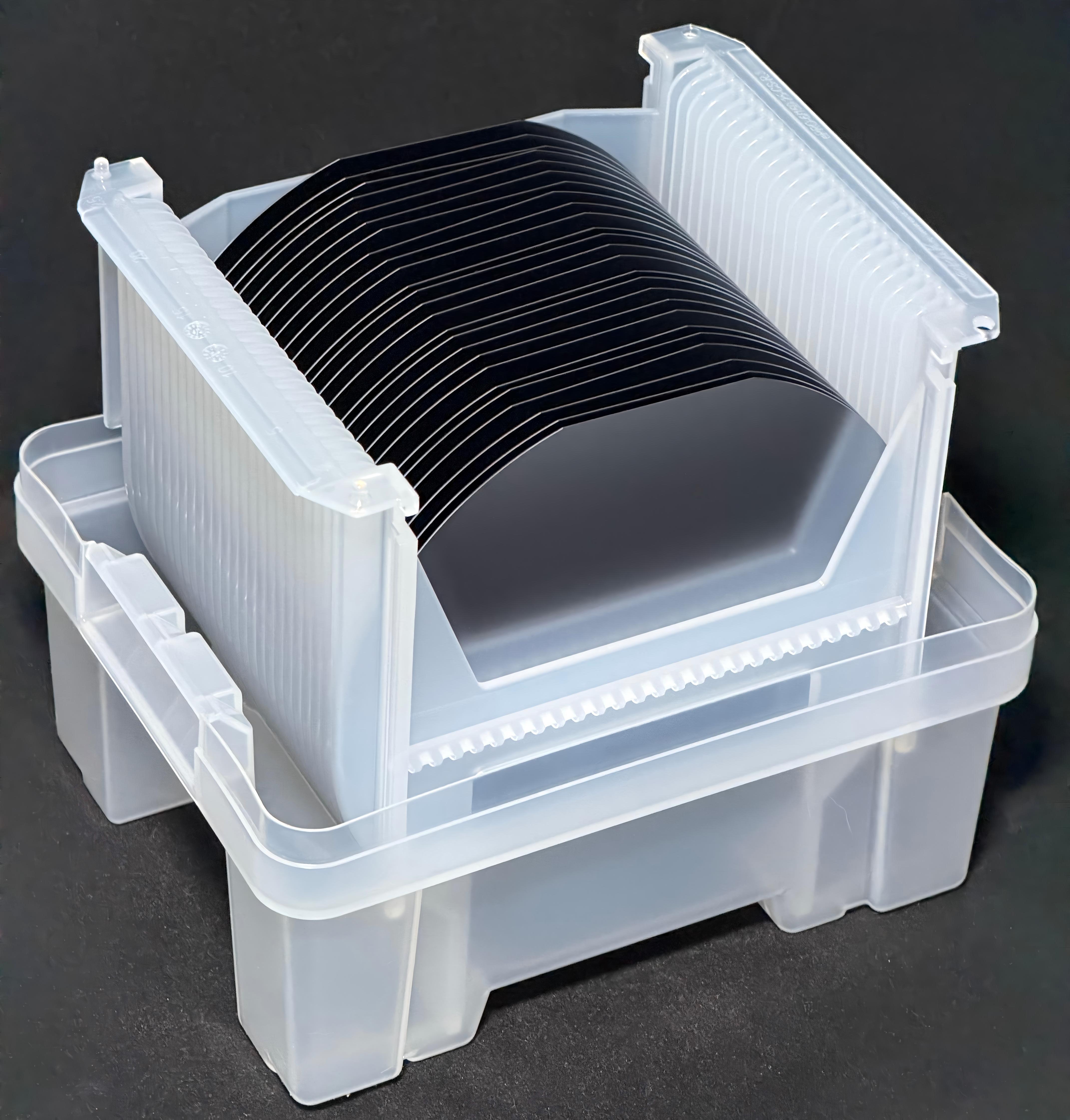
OMedaSemi provides silicon wafers. From 4inch to 12inch ,we have rich stock in 6inch 8inch and 12inch
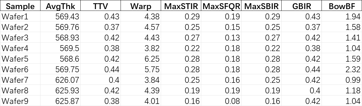
Below is the list of silicon wafer shipment test data from various major manufacturers we have compiled:
We can observe that as the wafer size increases, its roughness, TV, BOW, Wrap, and other indicators become more outstanding. This is because 12-inch and 8-inch FABs have stricter requirements for silicon wafers in consideration of yield, hence the production equipment for 12-inch and 8-inch silicon wafers also has higher precision.
 4inch MSK silicon wafer test data.xlsx
6inch YY silicon wafer test data.xlsx
8inch YY silicon wafer test data.xlsx
12inch ZH silicon wafer test data.xlsx
12inch ZX silicon wafer test data.xls
1. First, we introduce our featured products below, including
#Ultra-flat silicon wafer TTV<500nm
#High-resistance silicon wafer resistivity>10000ohm*cm
#Ultra-thin silicon wafer 8-inch thinnest 8um 12-inch thinnest 15um, and we can also undertake post-processing services such as thermal oxidation, coating, exposure, development, and etching
2. We usually use some common silicon wafer specifications when doing projects. We will display them below for you to choose. These silicon wafers can meet most needs and are all high-quality silicon wafers
**6-inch**
*6-inch low-resistivity silicon wafer 47.5 flat edge (57.5 flat edge optional) P100
6-inch low-resistivity silicon wafer 47.5 flat edge (57.5 flat edge optional) P100.pdf
*6inch High-resistivity(>10000ohm*cm) 47.5 flat edge (57.5 flat edge optional) P100
6inch High-resistivity(10000ohmcm) 47.5 flat edge (57.5 flat edge optional) P100.xlsx
**8-inch**
*8-inch low-resistivity silicon wafer notch P100
8-inch low-resistivity silicon wafer notch P100.pdf
*8inch High-resistivity(>10000ohm*cm) notch P100
8inch High-resistivity(10000ohmcm) notch P100.pdf
*8-inch heavily doped 0.002-0.004 ohm*cm, notch, N111 CZ
8-inch heavily doped 0.002-0.004 ohmcm, notch, N111 CZ.xlsx
Featured products:
#High-quality silicon wafers TTV<5um BOW WRAP<20um Ra<0.5nm
Can be directly used for 6-inch and 8-inch DUV stepper lithography machines to meet the stringent requirements for wafers
Can be directly used for various bonding requirements for wafers
#Provide ultra-flat silicon wafers comparable to Finland's OKemetics, and can mass-productation ultra-flat silicon wafers with TTV<500nm. The measured data are as follows
#Provide >10000ohm*cm FZ high-resistance silicon wafers for acoustic and electro-optic modulation applications
Can provide thermal oxidation high-resistance wafers with thermal oxidation and PolySi (Trap Rich Layer)
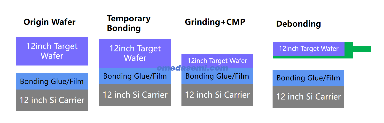
#Provide ultra-thin silicon wafers 8-inch thinnest 8um 12-inch thinnest 15um, using temporary bonding + debonding + thinning and polishing process to obtain ultra-thin silicon wafers
OMeda (Shanghai Omedasemi Co.,Ltd) was founded in 2021 by 3 doctors with more than 10 years of experience in nanpfabrication. It currently has 15 employees and has rich experience in nanofabrication (coating, lithography, etching, two-photon printing, bonding) and other processes. We support nanofabrication of 4/6/8-inch wafers.