Paper Download
 An Ultra-Broadband Photonic Chip-Based Parametric Amplifier.pdf
This paper describes the development of an ultra-broadband photonic-chip-based parametric amplifier (OPA) using gallium phosphide (GaP) on a silicon dioxide platform. Key highlights from the paper include:
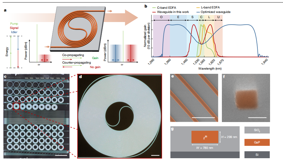
High Gain and Broadband Amplification: The OPA achieves a net gain of 25 dB, with an impressive bandwidth of up to 140 nm (17 THz), significantly outperforming traditional erbium-doped fiber amplifiers (EDFAs) in both gain and bandwidth.
Gallium Phosphide (GaP) Advantages: The use of GaP enables high optical nonlinearity and a high refractive index, making it ideal for parametric amplification. It mitigates issues like two-photon absorption and reduces device footprint by 60-fold compared to traditional systems.
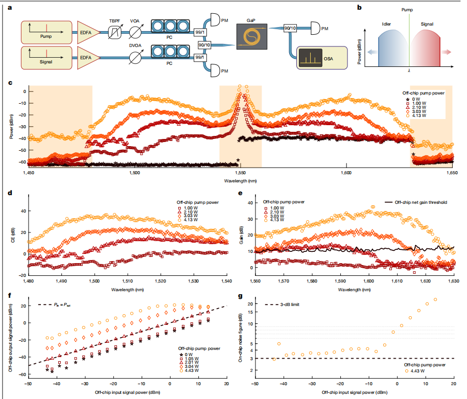
Amplification of Frequency Combs: The paper demonstrates that the OPA can amplify both narrowband electro-optic (EO) frequency combs and broadband dissipative Kerr soliton combs. The GaP OPA supports very weak signals, amplifying them by more than 20 dB, which is challenging for conventional EDFAs.
Applications in Coherent Communications: The amplifier was tested in a coherent communication setup, successfully amplifying a quadrature phase-shift keying (QPSK) encoded signal at 1,605 nm with a high dynamic range. This showcases the potential of the GaP OPA for modern telecommunication systems.
Reduced Noise Figure: The OPA demonstrated a noise figure of less than 4 dB, which is suitable for maintaining the integrity of transmitted signals over long distances.
Overall, the study highlights the potential of photonic integrated circuits (PICs) for next-generation optical amplification, providing a compact, scalable, and high-performance alternative to traditional fiber-based amplifiers .
OMeda (Shanghai Omedasemi Co.,Ltd) was founded in 2021 by 3 doctors with more than 10 years of experience in nanpfabrication. It currently has 15 employees and has rich experience in nanofabrication (coating, lithography, etching, two-photon printing, bonding) and other processes. We support nanofabrication of 4/6/8-inch wafers.