Paper Download
 Ge-on-insulator Platform for Mid-infrared Photonic Integrated Circuits.pdf
OMedaSemi develop 4-6 inch SICOI wafers (silicon carbide on insulator wafers). The wafers use Direct Bonding(hydropholic bonding) or surface activated bonding technology to bond thermal oxide wafers and 4H high-purity semi-insulating silicon carbide wafers together, and then control the thickness to the thickness you need through ion implantation, annealing, thinning or direct thinning and CMP polishing. It is worth noting that ion implantation and direct CMP and thinning have their own advantages and disadvantages.We also have a large stock available. You can visit this page to learn more:https://en.omedasemi.com/composite-wafer.html
The paper "Ge-on-insulator Platform for Mid-infrared Photonic Integrated Circuits" by Mitsuru Takenaka et al. explores the development of a germanium-on-insulator (GeOI) platform for mid-infrared (MIR) photonic integrated circuits (PICs).
Motivation & Background:
Mid-infrared (MIR) wavelengths are crucial for optical communication, sensing, and quantum information applications.
Silicon (Si) photonics is widely used for near-infrared (NIR) applications, but its transparency range is limited to 1.2–8 μm, restricting its use in MIR.
Germanium (Ge) is fully transparent in the 2–14 μm range, making it a promising alternative for MIR PICs.
Ge-on-Insulator (GeOI) Platform Development:
The paper introduces a GeOI platform where a thin Ge membrane is bonded onto a buried oxide (BOX) layer, enabling strong optical confinement.
Wafer bonding & Smart-cut techniques were used to fabricate GeOI wafers.
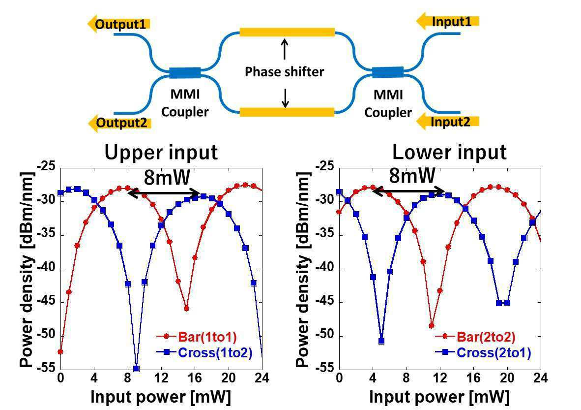
Key Devices Developed on GeOI:
Low-loss waveguides: Fabricated using optimized hydrogen ion implantation and annealing processes to minimize defects.
Thermo-optic (TO) phase shifters: Leveraging Ge’s higher thermo-optic coefficient (compared to Si) for efficient modulation.
Optical modulators: Utilizing free-carrier absorption in Ge for intensity modulation in the MIR range.
Photodetectors (PDs): A sub-bandgap Ge PD was developed, achieving high responsivity for MIR detection.
Performance & Applications:
Demonstrated compact and efficient PICs using GeOI for MIR optical sensing and communication.
The platform allows the integration of both passive and active components (waveguides, modulators, detectors) with low loss and high efficiency.
The GeOI platform provides a highly integrated and scalable solution for MIR photonics, leveraging existing silicon photonics technologies. The work demonstrates various essential photonic devices on GeOI, paving the way for next-generation MIR PICs for applications in sensing, communication, and computing.
Would you like a more detailed breakdown of specific sections?
OMeda (Shanghai Omedasemi Co.,Ltd) was founded in 2021 by 3 doctors with more than 10 years of experience in nanpfabrication. It currently has 15 employees and has rich experience in nanofabrication (coating, lithography, etching, two-photon printing, bonding) and other processes. We support nanofabrication of 4/6/8-inch wafers.