Paper Download
 Integrated Sub-Terahertz Cavity Electro-Optic Transduction.pdf
OMedaSemi can provide 4-inch and 8-inch LNOI wafers and LN-SOI
Application:
SAW surface acoustic wave device--POI wafer
TFLN PIC thin film lithium niobate photonic integrated circuit--LNOI wafer
Size: 4 inches 6 inches 8 inches
Crystal Orientation: X cut (for TFLN PIC), Y cut-Y128, Y36 (SAW), Z cut (SAW),LN-SOI
Processing technology: hydrophilic bonding + annealing, surface activation bonding
Customized processing: In addition to standard LNOI wafers, we also provide customized processing services for LNOI wafers.
Our advantages: full process and comprehensive processing capabilities
* Ion implantation * Thinning and polishing * Surface activation bonding * Hydrophilic bonding * Annealing * Ultra-high precision TRIM polishing Comprehensive processing capabilities can provide you with fast and efficient customized processing services.
We also have a large stock available. You can visit this page to learn more:https://en.omedasemi.com/linbo3_on_insulator.html
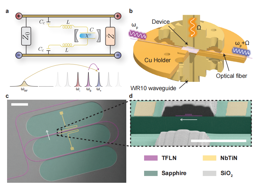
This article presents the development of an integrated electro-optic transducer operating in the sub-terahertz (sub-THz) frequency range, designed to bridge the gap between classical and quantum systems. The transducer combines a superconducting niobium titanium nitride (NbTiN) resonator at 107 GHz with a thin-film lithium niobate (TFLN) optical cavity to facilitate sub-THz to optical conversion.
Key findings include the achievement of photon transduction efficiency of approximately 0.82×10⁻⁶ and a single-photon electro-optic coupling rate of 0.7 kHz. The device leverages a triply-resonant electro-optic system where sub-THz signals modulate the refractive index of the TFLN, creating sidebands through three-wave mixing. The authors also address the challenges associated with integrated sub-THz resonators, such as parasitic modes from the sapphire substrate, and propose solutions to mitigate these effects.
The study also provides a detailed analysis of the device’s operation, including cryogenic optical and sub-THz cavity spectroscopy, and the characterization of the transduction efficiency as a function of optical and RF photon numbers. The results show a linear relationship between transduction efficiency and intracavity optical photon number, with some nonlinear effects attributed to local heating of the sub-THz resonator.
This work paves the way for future advancements in sub-THz quantum technologies by enabling high-efficiency electro-optic transduction and improving the integration of quantum devices across different frequency ranges.
OMeda (Shanghai Omedasemi Co.,Ltd) was founded in 2021 by 3 doctors with more than 10 years of experience in nanpfabrication. It currently has 15 employees and has rich experience in nanofabrication (coating, lithography, etching, two-photon printing, bonding) and other processes. We support nanofabrication of 4/6/8-inch wafers.