The article discusses the development of thick, hydrogenated amorphous silicon (a-Si:H) films that are crystallized for use as structural materials in the surface micromachining of MEMS inertial sensors. The research focuses on the electrical resistivity, mechanical stress, crystallinity, and surface roughness of a-Si:H layers, which are doped with phosphine (PH3) and annealed at various temperatures.
Key findings from the study include:
The deposition of thick a-Si:H layers using plasma-enhanced chemical vapor deposition (PECVD) results in varying film thickness and deposition rates based on PH3: H2 flow rates.
Crystallization at temperatures between 650°C and 900°C impacts the mechanical stress, with higher temperatures reducing tensile stress and improving the crystallinity.
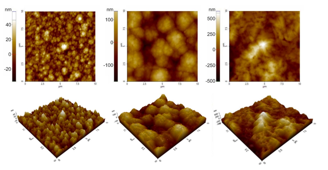
The surface roughness of crystallized a-Si:H layers is significantly smoother than that of epitaxial poly-Silicon (epi-poly Si), offering advantages in material savings and reduced processing time.
Electrical resistivity improves with higher crystallization temperatures, but excessive doping levels (high PH3: H2 flow rates) can lead to reduced conductivity.
The study also observes that the interaction between deposition parameters, annealing conditions, and material properties is complex, highlighting the need for optimization in MEMS applications.
In conclusion, the results suggest that carefully controlled deposition and annealing processes can enhance the performance of a-Si:H films, making them suitable for advanced MEMS sensor applications. Further research is needed to fully understand the mechanisms affecting crystallization and to optimize the processes for improved device fabrication.
OMeda (Shanghai Omedasemi Co.,Ltd) was founded in 2021 by 3 doctors with more than 10 years of experience in nanpfabrication. It currently has 15 employees and has rich experience in nanofabrication (coating, lithography, etching, two-photon printing, bonding) and other processes. We support nanofabrication of 4/6/8-inch wafers.