The paper discusses a novel monolithic 3D integration approach for integrating tantalum pentoxide (Ta₂O₅) photonics with arbitrary substrates, using thin-film lithium niobate (LN) as a substrate material. This integration aims to enable high-performance photonic systems that combine the benefits of both materials: Ta₂O₅ for nonlinear optics (χ(3) processes) and LN for second-order nonlinear optics (χ(2) processes).
Key points include:
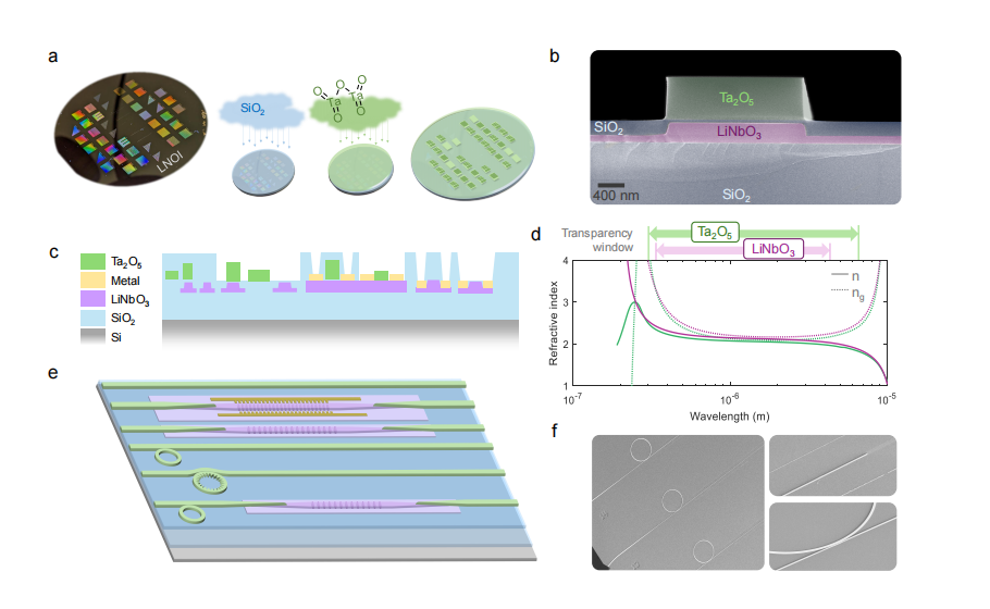
Monolithic 3D Integration: The study demonstrates the seamless integration of Ta₂O₅ photonics with LN using a room-temperature deposition method. This allows for the creation of photonic systems with enhanced capabilities, such as low-loss microresonators and nanophotonics, as well as quasi-phase-matching in LN for efficient nonlinear processes.
Nonlinear Optics: The integration facilitates several nonlinear processes, including optical parametric oscillation (OPO), soliton microcomb generation in Ta₂O₅, and second-harmonic generation (SHG) in LN. The integration of these processes into a single platform paves the way for more versatile and efficient photonic devices.
High-Quality Factors: The fabricated microresonators in the Ta₂O₅ layer exhibit very high quality factors (Q > 5 million), supporting efficient frequency conversion processes like OPO and SHG.
Efficient 3D Interlayer Routing: The monolithic design includes efficient interlayer routing between Ta₂O₅ and LN layers, making it possible to route light between the layers with minimal loss. This enables complex multi-functional devices in a single integrated system.
Applications: The paper outlines how the integration can lead to scalable, multifunctional photonic systems that support a wide range of applications, including quantum technologies, telecommunications, and visible-light photonics.
In conclusion, the monolithic 3D integration of Ta₂O₅ and LN offers a scalable platform for multifunctional photonic systems, enhancing existing photonic infrastructure with new nonlinear functionalities and high-performance capabilities.
OMeda (Shanghai Omedasemi Co.,Ltd) was founded in 2021 by 3 doctors with more than 10 years of experience in nanpfabrication. It currently has 15 employees and has rich experience in nanofabrication (coating, lithography, etching, two-photon printing, bonding) and other processes. We support nanofabrication of 4/6/8-inch wafers.