The article discusses the development of an isotropic atomic layer etching (ALE) process for MgO-doped lithium niobate (LiNbO₃ or LN), which is essential for improving the surface quality of thin-film lithium niobate (TFLN) devices used in photonic applications. The primary challenge addressed is the surface roughness and corrugations that lead to propagation losses in TFLN waveguides, which can hinder the performance of photonic devices, especially for quantum and nonlinear optics.
Key Points:
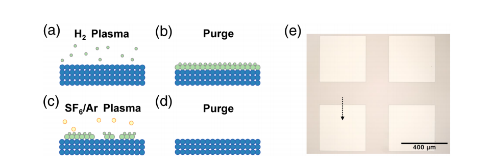
ALE Process Development: The authors present a sequential exposure process using hydrogen (H₂) and SF₆/Ar plasmas for isotropic ALE. The process achieved an etch rate of 1.59 nm/cycle with a synergy of 96.9%. The sequential nature of the process ensures self-limiting etching, which helps smooth the surfaces without significant loss of material, addressing issues such as sidewall roughness.
Substitute Recipes: The article explores alternative plasma combinations, such as SF₆/O₂ and Cl₂/BCl₃, to replace SF₆/Ar. The SF₆/O₂ combination showed a synergy of 99.5% and an etch rate of 2.24 nm/cycle, while Cl₂/BCl₃ achieved a synergy of 91.5%. These alternatives provide options for optimizing the ALE process for different conditions.
Surface Smoothing: The isotropic nature of ALE is crucial for smoothing sidewall roughness on TFLN waveguides, improving photonic performance. After 50 cycles of ALE, the sidewall roughness was reduced by 30%, and the process effectively smoothed the waveguide sidewalls when compared to traditional Ar⁺ milling techniques.
Characterization and Results: Atomic force microscopy (AFM) was used to measure etch depths and surface roughness. The surface roughness on bulk LN was initially 0.2 nm, and after 50 cycles of ALE, it improved to 0.57 nm, which suggests that the process is effective in smoothing the surfaces without significant etching damage. The lateral etch rate was found to be approximately 1 nm/cycle on waveguide sidewalls, confirming the isotropic nature of the etch.
X-ray Photoelectron Spectroscopy (XPS): XPS analysis was performed to understand the chemical composition changes before and after the ALE process. The results showed increased surface concentrations of lithium (Li), fluorine (F), and magnesium (Mg), likely due to the formation of LiF and MgF₂ during the etching process.
Potential for TFLN Devices: The ALE process could be used as a post-processing step after physical etching methods like Ar⁺ milling to reduce sidewall roughness and corrugations, improving the performance of TFLN-based nanophotonic devices. This is especially important for applications in nonlinear optics and quantum information processing.
Conclusion: The study introduces a successful isotropic ALE process for improving the surface quality of MgO-doped lithium niobate. The ability to reduce sidewall roughness and improve surface smoothness opens new possibilities for enhancing the performance of TFLN-based photonic devices, making them more suitable for high-performance quantum and nonlinear photonics applications.
OMeda (Shanghai Omedasemi Co.,Ltd) was founded in 2021 by 3 doctors with more than 10 years of experience in nanpfabrication. It currently has 15 employees and has rich experience in nanofabrication (coating, lithography, etching, two-photon printing, bonding) and other processes. We support nanofabrication of 4/6/8-inch wafers.