OMedaSemi develop a new process to fabricate ultra thin wafer ,this method can improve the mass production yield in mass production ,and can get thinner wafer compared with direct grinding and cmp,and for silicon wafer the thinnest that we can reach in 12 inch is 15um ,it is better than the report of Infineon 12 inch 20um.
We have use this method fabricate a lot of wafer ,if you have need about ultra thin wafer ,please share us your needs .
Material We support :
Lithium Niobate
Lithium Tantalate
Silicon
InP
SIlicon Carbide
Galium Oxide
SOI Wafer
Size We support: 12 inch max
Ultra-thin silicon wafers
A 6-inch silicon wafer/lithium niobate wafer was temporarily bonded and thinned. The top silicon layer was reduced to 21.2-22.2µm, with a TTV of 1.0µm.
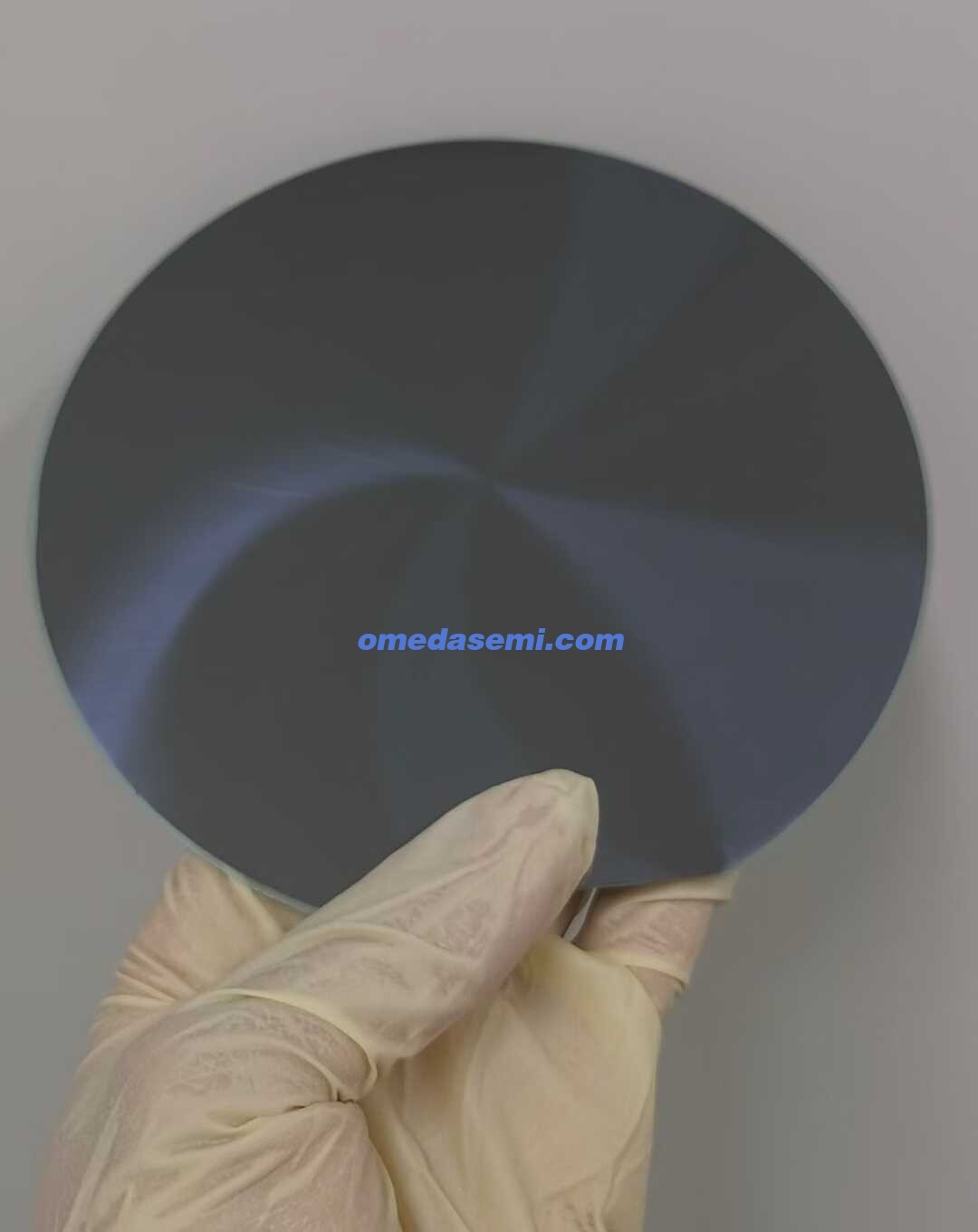
8-inch ultra-thin silicon wafer, thickness 6.5um, silicon and glass temporary bonding, TTv0.7um
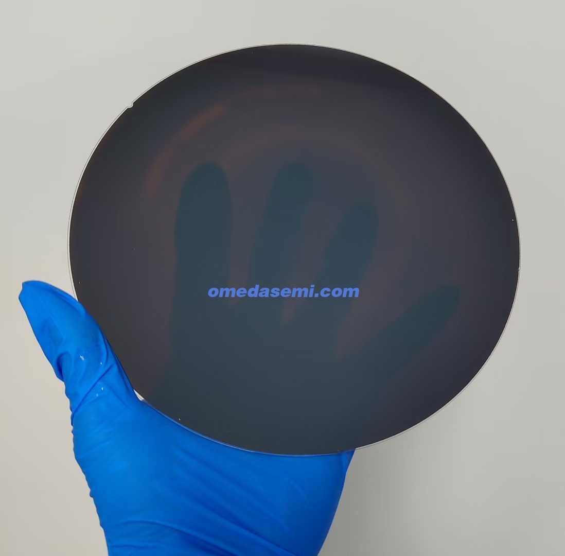
Temporary bonding of 12-inch silicon wafer and glass, thinning to 15um
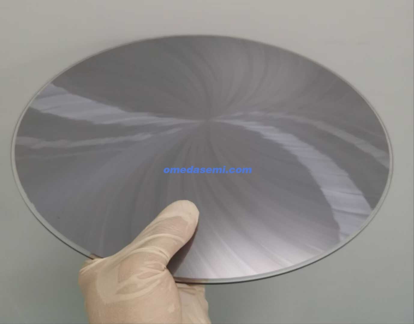
8-inch single crystal lithium niobate thinned to 8-20 microns (for PPLN devices and piezoelectric MEMS device applications)
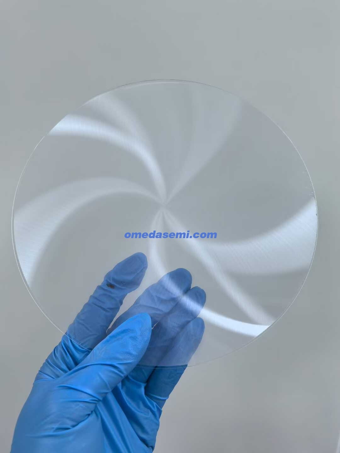
6-inch lithium tantalate thinned to 20-50 microns (for pyroelectric device applications)
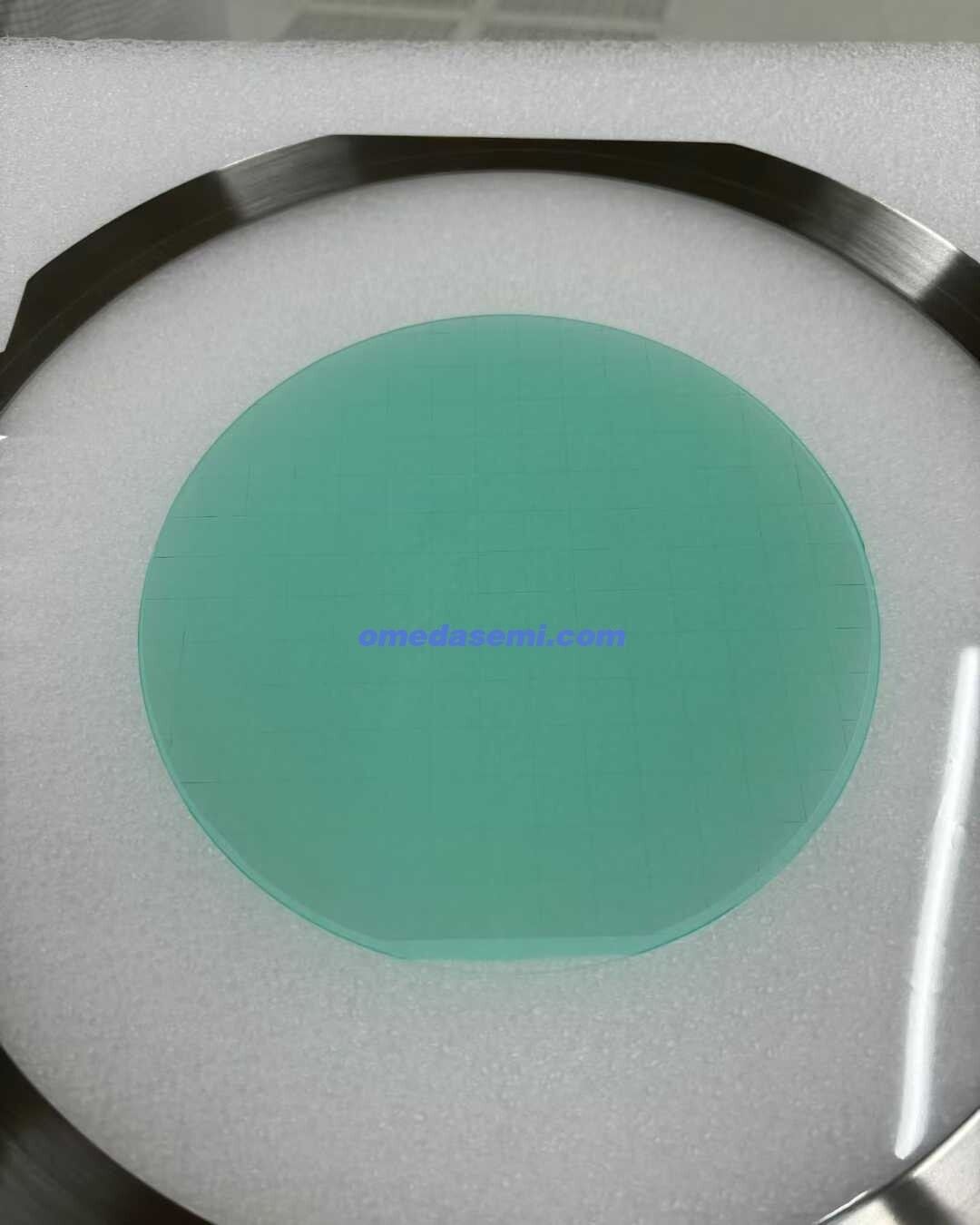
6-inch gallium oxide thinned to 30 microns (for heat dissipation of high-power devices)
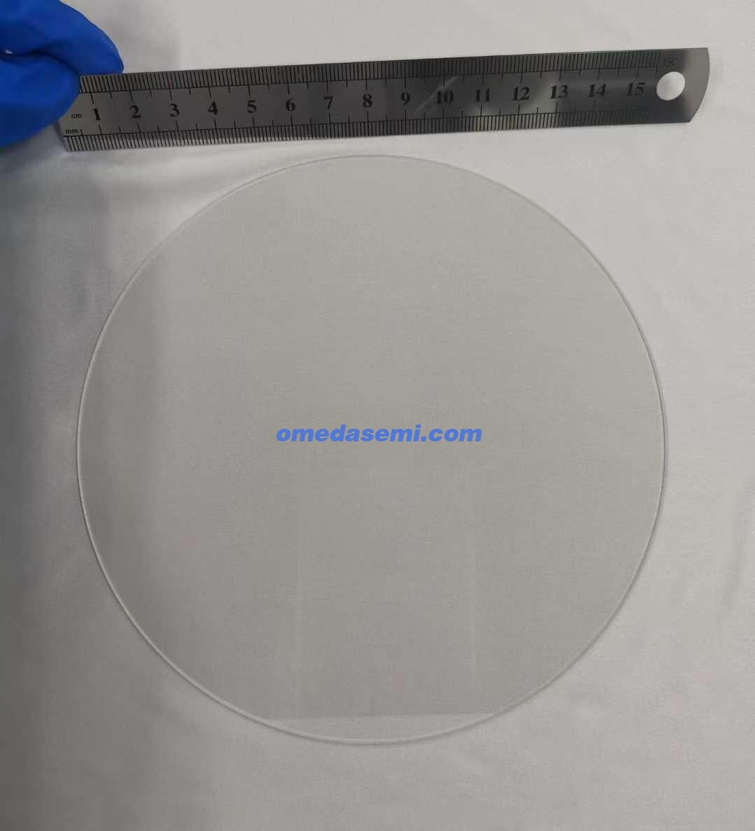
2-inch indium phosphide thinned to 20-50 microns (for heat dissipation of optoelectronic devices)
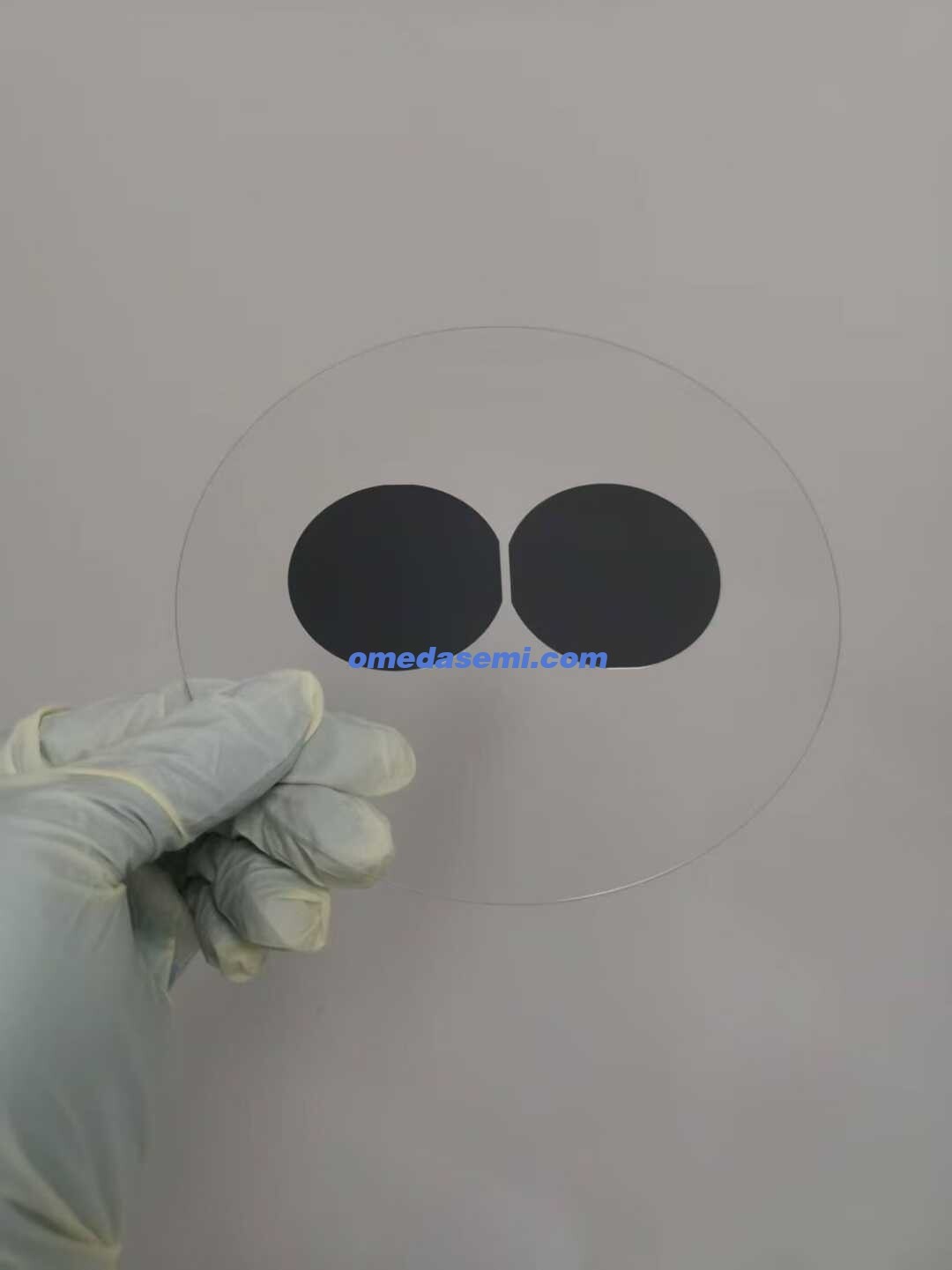
OMeda (Shanghai Omedasemi Co.,Ltd) was founded in 2021 by 3 doctors with more than 10 years of experience in nanpfabrication. It currently has 15 employees and has rich experience in nanofabrication (coating, lithography, etching, two-photon printing, bonding) and other processes. We support nanofabrication of 4/6/8-inch wafers.

