This paper focuses on the CMOS-compatible fabrication of superconducting qubits and their room-temperature (RT) characterization, which is a crucial step towards scalable quantum computing. It highlights a wafer-level characterization process for superconducting qubits on a 200-mm silicon wafer. The study outlines how detailed RT analysis can predict cryogenic performance and increase yield and frequency targeting for quantum processing units (QPUs).
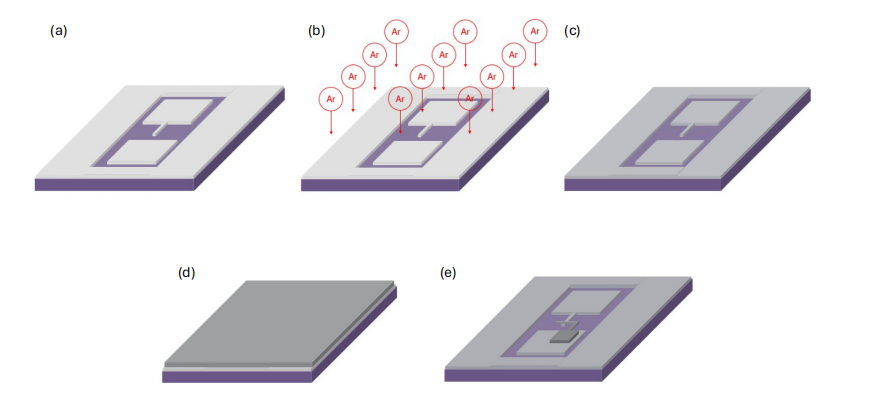
Wafer-Level Fabrication and Yield:
The fabrication approach is industry-grade and uses CMOS-compatible processing to manufacture superconducting qubits. The qubits are fabricated on a 200-mm wafer, achieving a yield of 92.8% across the wafer, with junction resistance spread (RSD) of 12.4% and variation in oxide barrier thickness of 7.2%.
The method includes the use of test structures like shorts and Josephson junctions (JJs) to analyze the variability and resistance spread across the wafer, ensuring that only functional devices are selected for the next processing stages.
Room-Temperature (RT) Characterization:
RT measurements are used for process monitoring and to predict the cryogenic behavior of the qubits. This allows for the preselection of functional qubits based on their resistance at RT, helping to exclude non-functional devices early in the fabrication process.
Key metrics like junction resistance and breakdown voltage are evaluated using current-voltage (IV) measurements, helping to assess the quality and reliability of the qubits before moving to low-temperature testing.
Cryogenic Characterization:
After selecting the qubits based on RT properties, low-temperature characterization is performed to confirm the qubits' frequency targeting, relaxation times (T1), and dephasing times (T2).
The best-performing qubits show T1 times up to 80 µs and T2 times greater than 100 µs, indicating high-quality qubits that meet the required performance for scalable quantum computing.
Methodology for Frequency Targeting:
The study uses the Ambegaokar-Baratoff relation to relate the RT resistance of Josephson junctions to the qubit frequency, enabling frequency prediction before the qubits are cooled to cryogenic temperatures.
Frequency spectroscopy and time-domain characterization are used to measure and calibrate qubit frequencies, demonstrating a frequency spread of 8.4% across the full 200-mm wafer.
Optimization and Process Control:
Process control monitoring (PCM) is integrated into the fabrication process, utilizing test junctions and shorts to assess critical parameters like the width variation of metal electrodes and the oxide barrier variation, which influence qubit performance.
This methodology optimizes the scalability of superconducting qubit production, helping to address frequency targeting challenges and improve yield.
This paper outlines an effective methodology for the industry-grade fabrication of CMOS-compatible superconducting qubits with a focus on scalability and wafer-level process control. The study demonstrates that room-temperature characterization of qubits during fabrication can significantly improve yield, frequency targeting, and overall performance. The results indicate the potential for large-scale quantum processors based on superconducting qubits, facilitating future advancements in quantum computing.
OMeda (Shanghai Omedasemi Co.,Ltd) was founded in 2021 by 3 doctors with more than 10 years of experience in nanpfabrication. It currently has 15 employees and has rich experience in nanofabrication (coating, lithography, etching, two-photon printing, bonding) and other processes. We support nanofabrication of 4/6/8-inch wafers.