Paper Download
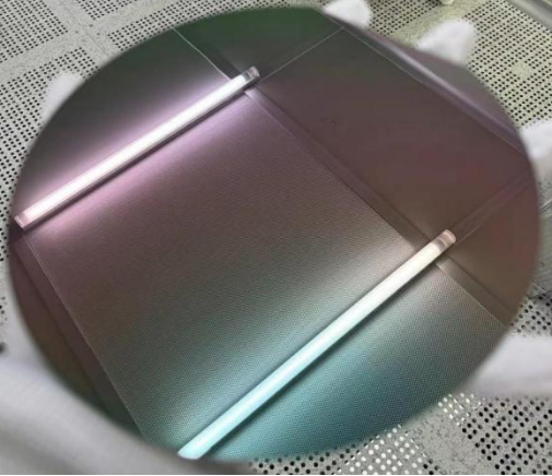
OMedaSemi can provide ultra low loss silicon nitride wafer , we use LPCVD/PECVD method to deposite Silicon Nitride film on thermal oxide wafer ,the film have good quality ,loss of thin film is 1dB/M,also the max size is 6 inch ,the max thickness is 800nm,we also have many stock ,you can visit this page to know more : Ultra Low Loss Silicon Nitride Thin Film Wafer

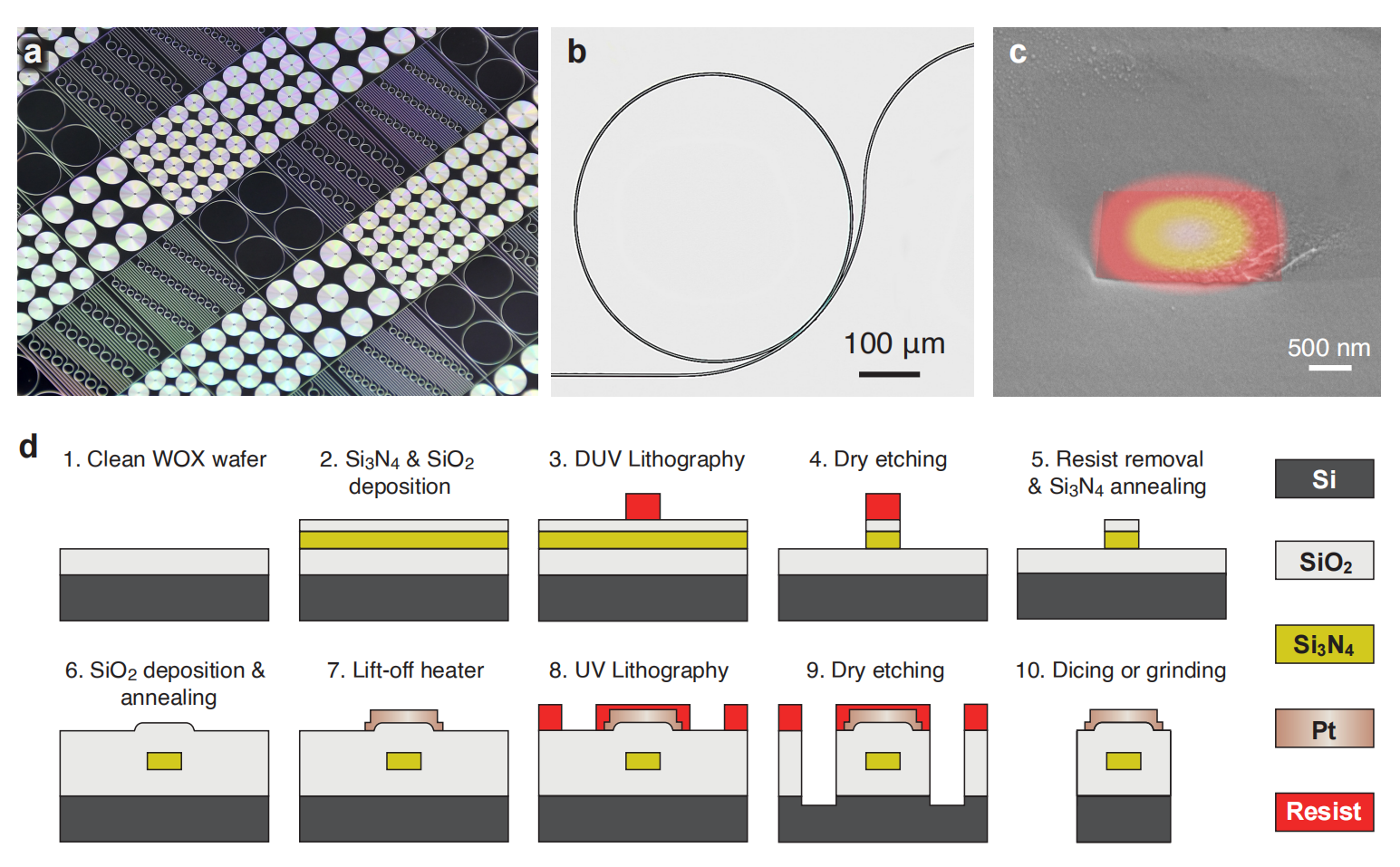
The article "LPCVD Si₃N₄ Foundry Manufacturing of Tight Confinement, Dispersion-Engineered, Ultralow-Loss Silicon Nitride Photonic Integrated Circuit" discusses the development of a fabrication process for silicon nitride (Si₃N₄) photonic integrated circuits (PICs) that achieves ultralow optical loss with tight confinement. The process uses low-pressure chemical vapor deposition (LPCVD) and advanced techniques to create PICs on 6-inch wafers, which is compatible with existing foundry standards.

Key points:
1. **Ultralow-Loss Achievement**: The paper reports an optical loss of 2.6 dB/m for Si₃N₄ waveguides, which is critical for applications like soliton microcomb generation.
2. **Process Scalability**: The fabrication process, involving deep-ultraviolet (DUV) stepper lithography and dry etching, is scalable from 6-inch to 8-inch wafers, offering high yield and uniformity across large-scale production.
3. **Applications**: The technology enables key advances in integrated photonics, such as the generation of Kerr frequency combs, optical communication, and quantum information processing. The tight optical confinement also allows for small mode volumes and bending radii, essential for high-performance devices.
This research pushes forward the commercial viability of Si₃N₄-based integrated photonic systems, which are increasingly relevant for telecommunications and data centers【11†source】.
OMeda (Shanghai Omedasemi Co.,Ltd) was founded in 2021 by 3 doctors with more than 10 years of experience in nanpfabrication. It currently has 15 employees and has rich experience in nanofabrication (coating, lithography, etching, two-photon printing, bonding) and other processes. We support nanofabrication of 4/6/8-inch wafers.