Paper Download

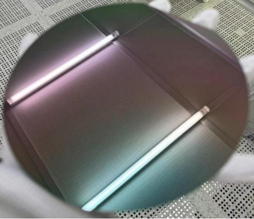
OMedaSemi can provide ultra low loss silicon nitride wafer , we use LPCVD/PECVD method to deposite Silicon Nitride film on thermal oxide wafer ,the film have good quality ,loss of thin film is 1dB/M,also the max size is 6 inch ,the max thickness is 800nm,we also have many stock ,you can visit this page to know more : Ultra Low Loss Silicon Nitride Thin Film Wafer

The article titled "Ultra-Low-Loss Silicon Nitride Photonics Based on Deposited Films Compatible with Foundries" focuses on the development of low-loss silicon nitride (Si₃N₄) photonic devices using foundry-compatible processes. Traditional methods for fabricating ultra-low-loss Si₃N₄ devices involve high-temperature deposition, which is unsuitable for foundries. This research presents a method to reduce propagation loss in Si₃N₄ waveguides deposited at low temperatures using plasma-enhanced chemical vapor deposition (PECVD).
Key points:
1. **Fabrication Process**: The process utilizes PECVD at 350°C to deposit Si₃N₄ films. Post-processing methods, such as chemical mechanical planarization (CMP) and rapid thermal anneal (RTA), are employed to reduce surface roughness and improve film quality. Surface roughness is decreased from 1.36 nm to 0.20 nm after CMP.

2. **Loss Reduction**: Without annealing, the waveguides have a propagation loss of 0.42 dB/cm. After RTA, the loss reduces to 0.28 dB/cm, and furnace annealing achieves an even lower loss of 0.06 dB/cm, comparable to high-temperature methods.
3. **Applications**: These low-loss waveguides can be used for both linear and nonlinear applications, such as low-threshold parametric oscillation, broadband frequency comb generation, and narrow-linewidth lasers.
4. **Conclusion**: The study demonstrates that ultra-low-loss Si₃N₄ photonic devices can be fabricated using foundry-compatible processes, enabling scalable photonic systems. The research offers a pathway for integrating photonics with electronics, pushing the limits of system-level innovation.
The work is a promising advancement in photonic integration, especially for industries relying on foundry-compatible processes.
OMeda (Shanghai Omedasemi Co.,Ltd) was founded in 2021 by 3 doctors with more than 10 years of experience in nanpfabrication. It currently has 15 employees and has rich experience in nanofabrication (coating, lithography, etching, two-photon printing, bonding) and other processes. We support nanofabrication of 4/6/8-inch wafers.