Paper Download

OMedaSemi provide Two Photon 3D Printing Service,we use Nanoscribe Phtonics GT2 Pro & Nanoscribe Quantum X and Nanoscribe IP Dip Glue to print nanostructure on most of substrate(Glass Silicon Fiber) ,you can visit this page to know more : Two Photo Polymerization 3D Printing Service
The article presents a new method for designing and fabricating high numerical aperture (NA) achromatic metalenses using 3D-printed multilayer structures. Metalenses, which are flat optical devices made from nanostructures, are known for their compactness and efficiency but often suffer from chromatic aberration and performance trade-offs between NA and bandwidth. These limitations restrict their use in broadband applications.

Key Contributions:
Challenges with Traditional Metalenses: Most conventional metalenses are highly dispersive, meaning they only function efficiently at specific wavelengths, especially those made with high-refractive-index materials. Achromatic lenses can correct for chromatic aberration, but combining high NA and broad bandwidth remains difficult.
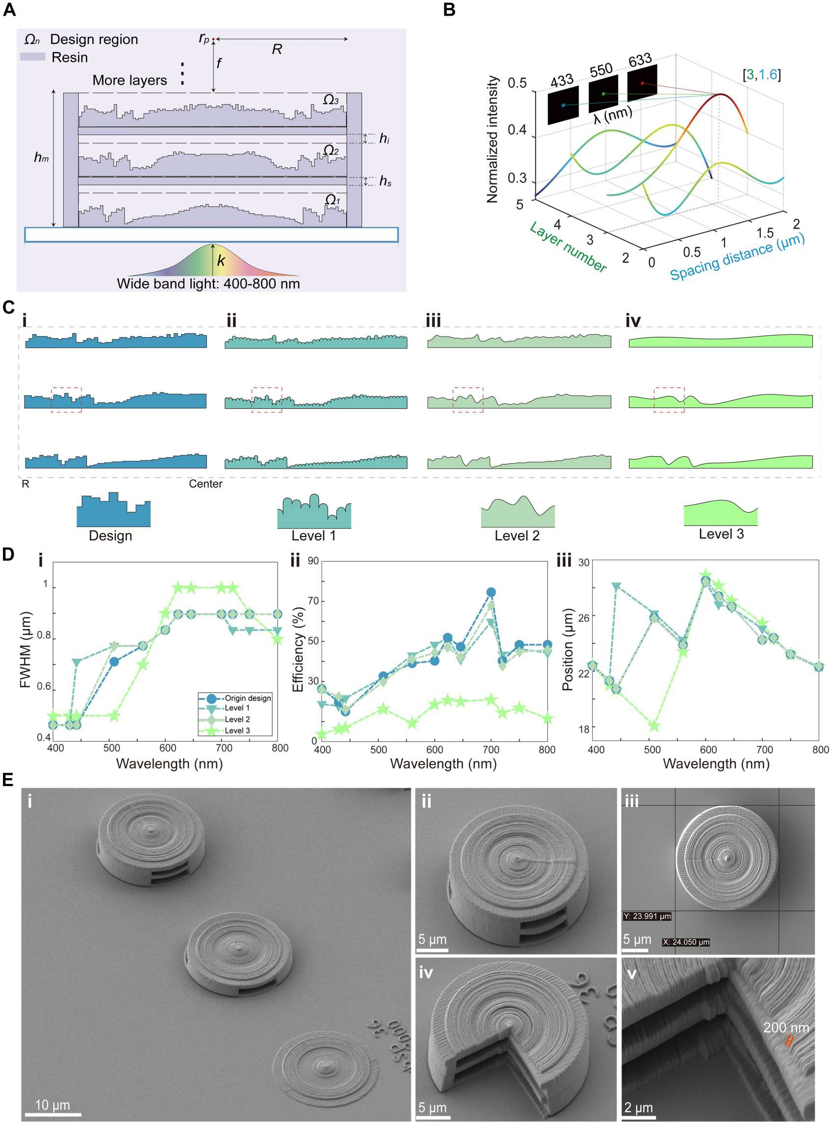
3D Printing as a Solution: The authors propose a solution using 3D-printed multilayer achromatic metalenses (MAMs) fabricated through two-photon polymerization lithography (TPL). This technique allows for precise, high-resolution structures to be created in a low-refractive-index polymer, overcoming the limitations of high-index materials.
Design Optimization: By employing topology optimization (TO), the team uses inverse design methods to configure the heights and distances of nanostructures in multiple layers, optimizing the MAMs for both high NA and broadband performance. They tested designs with numerical apertures of 0.5 and 0.7.
Results: The MAMs created in the study measured 20 μm in diameter, operated in the visible light spectrum (400-800 nm), and achieved high efficiencies (up to 42%). They demonstrated broadband imaging with minimal chromatic aberration, under both white light and RGB illumination, proving the effectiveness of the design in overcoming traditional limitations.
Impact and Applications: The study highlights the potential of these 3D-printed multilayer structures to significantly improve the performance of meta-optical devices, with applications in imaging, quantum technology, and bioanalysis. The results pave the way for the development of high-performance, multifunctional photonic devices that are both broadband and polarization-insensitive.
In conclusion, the research showcases how 3D printing and inverse design techniques can revolutionize the fabrication of advanced optical devices like metalenses, overcoming traditional performance constraints.
OMeda (Shanghai Omedasemi Co.,Ltd) was founded in 2021 by 3 doctors with more than 10 years of experience in nanpfabrication. It currently has 15 employees and has rich experience in nanofabrication (coating, lithography, etching, two-photon printing, bonding) and other processes. We support nanofabrication of 4/6/8-inch wafers.