Paper Download

OMedaSemi provide Two Photon 3D Printing Service,we use Nanoscribe Phtonics GT2 Pro & Nanoscribe Quantum X and Nanoscribe IP Dip Glue to print nanostructure on most of substrate(Glass Silicon Fiber) ,you can visit this page to know more : Two Photo Polymerization 3D Printing Service
The article discusses the development of a novel optical fiber microphone based on a 3D-printed microcantilever structure, fabricated using two-photon polymerization (TPP) technology. The goal is to create a highly sensitive microphone that operates efficiently within the human audible frequency range (20 Hz to 20 kHz), achieving a signal-to-noise ratio (SNR) of over 50 dB.
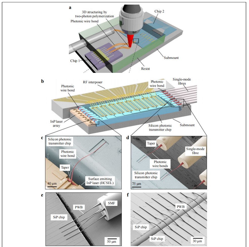
The article "Two-photon lithography for integrated photonic packaging" reviews the use of two-photon lithography (TPL) as an emerging solution for addressing the challenges in photonic integrated circuits (PICs) packaging. While PICs have made significant advances in optical communication and related technologies, their packaging remains complex due to the need for extremely precise optical alignment, which current electronic packaging methods cannot handle.

Challenges in Photonic Packaging:
PICs packaging demands higher precision compared to electronic packaging, requiring sub-micron alignment tolerances.
Heterogeneous integration, where different material platforms (e.g., silicon, III-V, lithium niobate) are combined, adds complexity to photonic packaging.
Two-photon Lithography (TPL):
TPL is a laser-based 3D printing technique that allows for precise fabrication of sub-micron structures by using a laser to solidify a photopolymer material.
TPL offers deep subwavelength resolution, making it ideal for photonic packaging, enabling flexible and custom designs for optical connections and micro-optical elements.
Advantages of TPL for Photonic Packaging:
Optical connections: TPL can be used to create optical links between photonic components after assembly, relaxing the alignment tolerances and allowing for standard electronic assembly techniques.
Microoptics and freeform optics: TPL allows for the integration of microoptical elements to direct and couple light more efficiently within photonic systems.
Hybrid integration: It can create interconnections between different optical materials and platforms, facilitating the use of hybrid integrated systems.
Mechanical alignment structures: TPL can also fabricate microstructures that assist in the precise passive alignment of components during packaging.
Applications and Future Directions:
TPL is seen as a promising technology for scaling up the production of integrated photonic systems by overcoming current packaging limitations.
The paper highlights future research directions, including improving the resolution and speed of TPL systems and expanding its application to more material systems and hybrid photonic devices.
In conclusion, the article emphasizes the potential of TPL to revolutionize the packaging of photonic integrated circuits, offering solutions to both optical alignment challenges and enabling the integration of complex multi-material systems.
OMeda (Shanghai Omedasemi Co.,Ltd) was founded in 2021 by 3 doctors with more than 10 years of experience in nanpfabrication. It currently has 15 employees and has rich experience in nanofabrication (coating, lithography, etching, two-photon printing, bonding) and other processes. We support nanofabrication of 4/6/8-inch wafers.