Paper Download

OMedaSemi use SAB Bonding Methond to bonding most of material,Surface activated bonding (SAB) is a room temperature wafer bonding technique with an atomically cleaned and activated surface. Surface activation is usually performed prior to bonding using rapid atomic bombardment to clean the surface. High strength bonds between semiconductors, metals, and dielectrics can be obtained even at room temperature.This bonding method can bond most of material ,such as Diamond, Sic,GaN,LiNbO3,Glass,Silicon,Sapphire,Inp,GaAs. if you want to know more ,please visit this page:Surface Actived Bonding Technology
The article titled "Room Temperature Wafer Bonding of Glass Using Aluminum Oxide Intermediate Layer" explores a novel method for bonding glass substrates at room temperature using an aluminum oxide (AlO) intermediate layer. This method is particularly valuable for applications where trKey Points:

Traditional Challenges in Glass Bonding:
Traditional glass bonding methods often require high-temperature annealing, leading to thermal stress and potential damage to heat-sensitive components.
Common adhesives, like epoxies, can degrade optical transparency and allow water permeation, making them unsuitable for optical applications.
Room Temperature Bonding via Surface Activated Bonding (SAB):
SAB is a technique used for room temperature bonding of inorganic materials by treating surfaces with ion beams to activate bonding.
Previous SAB approaches using silicon (Si) as an intermediate layer caused optical degradation, reducing transparency and limiting their usefulness for optical devices.
Innovation with Aluminum Oxide (AlO):
The authors propose using an AlO intermediate layer instead of Si to improve transparency and bonding strength.
The AlO layer is deposited using ion beam sputtering, and bonding is activated with an argon ion beam, resulting in a strong bond without the need for high temperatures.
Bond Strength and Optical Performance:
The bonding using the AlO layer achieved a bond strength of 1.32 J/m², which is suitable for wafer processing.
Optical tests demonstrated that the AlO layer did not degrade the transparency of the bonded interface, maintaining excellent transmittance and reflectance comparable to unbonded glass.
Comparison with Silicon-Based Bonding:
Glass bonded with Si intermediate layers exhibited significant losses in transparency, with a notable increase in reflectance (up to 38% at 400 nm wavelength), making it unsuitable for optical devices.
In contrast, the AlO layer preserved the glass's optical properties, making it ideal for applications requiring high transparency.
Microscopic and Chemical Analysis:
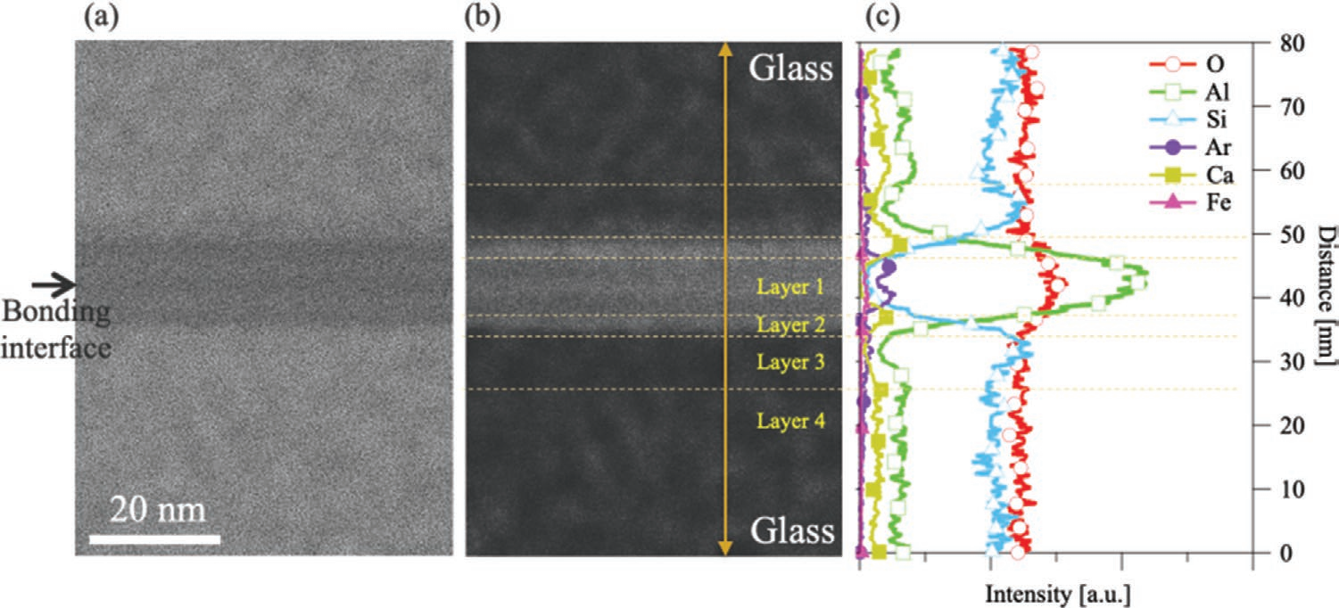
The study used XPS and STEM-EDX analyses to investigate the bonding mechanism, revealing that the AlO interface was amorphous and oxygen-deficient, which contributed to strong bonding without requiring high temperatures.
The AlO intermediate layer showed a more uniform structure compared to the Si-based bonding, which had a more complex layered structure and localized impurities.
The room temperature wafer bonding method using an AlO intermediate layer developed in this study provides a promising solution for bonding glass substrates while maintaining transparency and bond strength. This method is particularly well-suited for optical and microfluidic applications, overcoming the limitations of traditional high-temperature bonding techniques and Si-based intermediate layers.
OMeda (Shanghai Omedasemi Co.,Ltd) was founded in 2021 by 3 doctors with more than 10 years of experience in nanpfabrication. It currently has 15 employees and has rich experience in nanofabrication (coating, lithography, etching, two-photon printing, bonding) and other processes. We support nanofabrication of 4/6/8-inch wafers.