This paper presents a method for the precise measurement of the dynamic frequency of frequency-modulated lasers (FMLs) using integrated lithium niobate electro-optic frequency combs. The approach is designed to track the absolute frequency of FMLs with a chirp rate as high as 2×10^18 Hz/s, which is over three orders of magnitude faster than previous methods.
Key findings include:
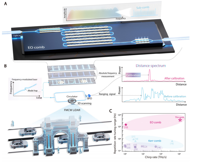
High-Speed Frequency Measurement: The dual electro-optic combs enable high-precision, real-time measurement of FML’s absolute frequency, achieving an acquisition rate of 10 GHz, allowing for accurate tracking of FMLs with high chirp rates.
Mode-Hop Frequency Modulated Lasers: The method can track FMLs with mode hops, a significant challenge in applications like frequency-modulated continuous-wave (FMCW) LiDAR. This allows for unambiguous distance measurement even with mode-hop FMLs, providing high ranging resolution.
3D Imaging Application: The system was used in FMCW LiDAR to generate high-precision 3D point clouds from real-world targets at a distance of 20 meters. The method successfully reconstructed the FMCW signal, demonstrating the potential for FMCW LiDAR to work with mode-hop FMLs.
Device Design: The electro-optic comb was designed using phase modulators and an amplitude modulator to create a broadband, flat-top spectrum with a tunable repetition rate. The device enables real-time tracking and calibration of FMLs with various chirp rates.
Broader Implications: The technique has wide-ranging applications in high-precision measurement of frequency, distance, and time, with potential in areas like spectroscopy, telecommunications, and biomedical science.
The paper demonstrates a groundbreaking approach to fast and accurate absolute frequency measurement, offering substantial improvements over current technologies and enabling advanced applications in precise laser-based ranging systems.
OMeda (Shanghai Omedasemi Co.,Ltd) was founded in 2021 by 3 doctors with more than 10 years of experience in nanpfabrication. It currently has 15 employees and has rich experience in nanofabrication (coating, lithography, etching, two-photon printing, bonding) and other processes. We support nanofabrication of 4/6/8-inch wafers.